Note : Les descriptions sont présentées dans la langue officielle dans laquelle elles ont été soumises.
CA 02454743 2004-O1-22
WO 03/012885 PCT/US02/20965
1
METHODS FOR PRODUCING ELECTROLUMINESCENT
DEVICES BY SCREEN PRINTING
This application claims the benefit of U.S. Provisional Application Serial No.
60/308,276, filed on July 27, 2001, which is incorporated herein by reference.
The present invention arose through work supported in part by Office of Naval
Research. The United States Government may have certain rights to this
invention
under 35 U.S.C. Section 200 et seq.
Technical Field of the Invention
This invention relates to light-emitting devices driven by an electric field
and
which are commonly referred to as electroluminescent devices.
Background of the Invention
Conjugated polymers have proven to be excellent candidates for low cost
large area display applications, due to unique properties such as
electroluminescence (EL), solution processibility, band gap tunability and
mechanical flexibility. A major advantage of the conjugated polymer light
emitting
devices (LEDs) is their potential capability of using web based roll-to-roll
processing.
If realized, the manufacturing cost of polymer LEDs for large area
applications may
be significantly reduced. In the past few years, polymer LEDs have made
remarkable progress toward commercialization, though the effort is mainly
focused
on small-area applications.
RECTIFIED SHEET (RULE 91)
CA 02454743 2004-O1-22
WO 03/012885 PCT/US02/20965
2
Typical single layer polymer LEDs are constructed by sandwiching a thin layer
of luminescent conjugated polymer between two electrodes, an anode and a
cathode, where at least one of the electrodes is either transparent or
semi-transparent. In some multilayer devices, charge injection and transport
layers
may be incorporated to improve the device performance. For selected multilayer
devices, electrons and holes combine at the interfaces to form exciplexes that
emit
light of a different color than either of the polymers comprising the
interface. When a
high electric field is applied between the electrodes in these devices,
electrons are
injected from the cathode and holes injected from the anode into the polymer
layers.
The injected charges recombine and decay radiatively to emit light. The double
charge injection mechanism of such polymer LEDs requires matching of the
cathode
(anode) work function to the corresponding LUMO (HOMO) level of the polymer
with
which the electrode is in contact, in order to achieve efficient charge
injection.
Indium-tin-oxide (1T0) is widely used as the anode material for polymer LEDs
because it is conductive, transparent and has a relatively high work function
that is
close to the HOMO level of many conjugated polymers. Because most conjugated
polymers have relatively low electron affinity, however, they require metals
with low
work functions as the cathode material to achieve efficient electron
injection. Low
work function metals are generally oxygen reactive, leading to which are
usually
unstable. Devices with low work function cathodes may even degrade during
storage.
In a typical polymer LED, the polymer layers are formed by spin-casting or
other similar techniques, such as dip-coating, that are more suitable for
large area
processing. The cathode, on the other hand, is almost exclusively formed by
vacuum
CA 02454743 2004-O1-22
WO 03/012885 PCT/US02/20965
3
deposition techniques such as thermal evaporation or sputtering of low work
function
metals or alloys. These vacuum deposition techniques are expensive, slow, and
not well
suited for large area processing.
It is thus an object of the present invention to provide a method of
fabrication
that provides a fast, inexpensive means of fabricating polymer light emitting
devices
suitable for large area applications.
Although described with respect to the field of light-emitting devices driven
by
an electric field, it will be appreciated that similar advantages of fast,
inexpensive
fabrication, as well as other advantages, may obtain in other applications of
the
present invention. Such advantages may become apparent to one of ordinary
skill in
the art in light of the present disclosure or through practice of the
invention.
Summary of the Invention
The present invention includes electroluminescent polymer devices and
electroluminescent polymer systems. The present invention also includes
machines
and instruments using those aspects of the invention. Included in the present
invention are methods for the fabrication of such devices by screen printing.
The
methods of the present invention may be applied using procedures and protocols
known and used in the arts to which they pertain. The methods of the present
invention may be used to manufacture unipolar LED devices, bipolar SCALE
devcies
and bipolar two-color SCALE devices. The present invention may be used to
upgrade, repair, or retrofit existing machines or instruments using those
aspects of
the invention, using methods and components used in the art.
CA 02454743 2004-O1-22
WO 03/012885 PCT/US02/20965
4
Method for preparing a layered composite
In broadest terms, the method of the present invention for preparing a layered
composite capable of forming a light-emitting device comprises the steps of:
(1)
obtaining a substrate material comprising a layer of an electrode material;
(2)
forming an emitting layer on the substrate material, the emitting layer
capable of
functioning as a light-emitting layer in a light-emitting device; and (3)
applying a
conductive paste material to the emitting layer, such as silver paste, the
conductive
paste material comprising a layer of an electrode material. The emitting layer
may
also be coated with an appropriate buffer layer prior to application of said
conductive
paste material, such as a layer of an appropriate semiconducting or conducting
polymer.
The conductive paste material may applied by a technique such as painting,
spraying, or screen-printing. The substrate material may consist of a material
such
as flexible ITO-coated PET or ITO-coated glass, thus the substrate may be
either
flexible or rigid. The substrate material may also be substantially
impermeable to
either oxygen or water. The emitting layer may be selected from the group
consisting of light emitting molecules, oligomers, polymers, their derivatives
and
blends thereof. Further the emittng layer may itself be comprised of multiple
layers.
In the case of a multi-layered emitting layer, each sub-layer of the multi-
layerd
emitting layer may be separately chosen from light emitting molecules,
oligomers
and polymers. The semiconducting and conducting polymers may be selected from
the group consisting of polyanilines, polythiophenes, polypyrroles, their
derivatives,
their copolymers and blends thereof.
CA 02454743 2004-O1-22
WO 03/012885 PCT/US02/20965
The electrodes of the present invention may be patterned, such as for
pixelation.
Examples of conductive pastes that may be used in the present invention
include: silver paste, gold paste, graphite paste, carbon paste or other
particulate
conductors dispersed in a medium allowing it to be applied by printing or
screen
printing technologies.
Examples of light emitting molecules that may be used in the emitting layer
include: tris(8-quinolinolato)aluminum, bis(2-(2-
hydroxyphenyl)pyridinato)beryllium,
anthracene, tris(2-phenylpyridine)iridium doped in a host of 4,4'-N,N'-
dicarbazol-
biphenyl, their derivatives and blends thereof.
Examples of light emitting oligomers that may be used in the emitting layer
include: oligo(phenylenevinylene)s, sexithiophene, oligo(thiophene)s,
oligo(pyridine)s, their derivatives and blends thereof.
Examples of light emitting polymers that may be used in the emitting layer
include: poly(arylene vinylene)s, poly(phenylene)s, poly(fluorene)s, polyvinyl
carbazole), poly(pyridine), poly(pyridyl vinylene), poly(phenylene vinylene
pyridyl
vinylene), their derivatives, their copolymers and blends thereof.
La rLered composite
Also included in the present invention is, in broadest terms, a layered
composite capable of forming a light-emitting device comprising: (1) a
substrate
material comprising a layer of an electrode material; (2) an emitting layer
formed on
the substrate material, the emitting layer capable of functioning as a light-
emitting
layer in a light-emitting device; and (3) a conductive paste material such as
silver
CA 02454743 2004-O1-22
WO 03/012885 PCT/US02/20965
6
paste applied to the emitting layer, the conductive paste material comprising
a layer
of an electrode material. The layered composite may additionally comprise an
appropriate buffer layer between the emitting layer and the conductive paste
material. The buffer layer may be selected from the group consisting of
semiconducting and conducting polymers.
The conductive paste material of the layered composite may be applied by a
technique such as painting, spraying, or screen-printing. The substrate
material may
be selected from the group consisting of flexible ITO-coated PET and ITO-
coated
glass. The substrate material may also be substantially impermeable to either
oxygen or water. The emitting layer may be selected from the group consisting
of
light emitting molecules, oligomers and polymers, their derivatives, coplymers
and
blends such as PPV, PPyVPV, PTP and poly(flourene)s. The semiconducting and
conducting polymers may be selected from the group consisting of polyanilines,
polypyrroles or blends of PPyVPV and PTP.
The electrodes of the present invention may be patterned, such as for
pixelation.
Examples of conductive pastes that may be used in the present invention
include: silver paste, gold paste, graphite paste, carbon paste or other
particulate
conductors dispersed in a medium allowing it to be applied by printing or
screen
printing technologies.
Examples of light emitting molecules that may be used in the emitting layer
include: tris(8-quinolinolato)aluminum, bis(2-(2-
hydroxyphenyl)pyridinato)beryllium,
anthracene, tris(2-phenylpyridine)iridium doped in a host of 4,4'-N,N'-
dicarbazol-
biphenyl, their derivatives and blends thereof.
CA 02454743 2004-O1-22
WO 03/012885 PCT/US02/20965
7
Examples of light emitting oligomers that may be used in the emitting layer
include: oligo(phenylenevinylene)s, sexithiophene, oligo(thiophene)s,
oligo(pyridine)s, their derivatives and blends thereof.
Examples of light emitting polymers that may be used in the emitting layer
include: poly(arylene vinylene)s, poly(phenylene)s, poly(fluorene)s, polyvinyl
carbazole), poly(pyridine), poly(pyridyl vinylene), poly(phenylene vinylene
pyridyl
vinylene), their derivatives, their copolymers and blends thereof.
Brief Description of the Drawings
Figure 1 shows repeat units of the materials of the present invention: (a)
poly(pyridyl vinylene phenylene vinylene) (PPyVPV); (b) poly(thienylene
phenylene)
(PTP); (c) sulfonated polyaniline (SPAN).
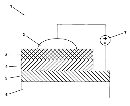
Figure 2 is a side elevational view of a polymer light-emitting device using
silver
paste as the top electrode in accordance with one embodiment of the present
invention.
Figure 3 shows the current-voltage and luminance-voltage characteristics for
the
ITO/PPyVPV:PTP/silver paste device of the present invention.
Figure 4 shows a variation of the EL intensity (solid line) with time of a
ITO/PPyVPV:PTP/silver paste device of the present invention.
Detailed Description of the Preferred Embodiments
CA 02454743 2004-O1-22
WO 03/012885 PCT/US02/20965
8
In accordance with the foregoing summary, the following present a detailed
description of the preferred embodiment of the invention that is currently
considered
to be the best mode.
The present invention presents a method for the fabrication of working light-
emitting devices using silver paste as the cathode. This may be made possible
by
the presence of a buffer layer comprised of a semiconducting polymer (such as
the
emeraldine base form of polyaniline) or a conducting polymer, such as
sulfonated
polyaniline (SPAN). To eliminate the use of low work function metals, one may
either
use polymers with high electron affinities or modify the charge injection
characteristics at the polymer/electrode interfaces.
Along these lines, a preferred embodiment of the present invention utilizes
pyridine containing conjugated polymers and copolymers (which have higher
electron affinities than their phenyl analogs) as the emitting materials and
novel
device configurations such as symmetrically configured AC light-emitting
(SCALE)
devices. These devices may modify the charge injection and/or transport
characteristics such that their operations are insensitive to the electrode
materials
used. As a consequence, more stable metals such as AI or Au may be used as
electrodes.
Using the novel structure of SCALE devices with a structure of
substrate/ITO/emitting layer/SPAN, the top electrode may be formed simply by
painting the silver paste over the SPAN layer. This may allow a very
inexpensive and
fast means to form a stable top electrode. When high resolution is needed, the
electrode may be formed by screen printing techniques. Unlike the vacuum
CA 02454743 2004-O1-22
WO 03/012885 PCT/US02/20965
9
deposition techniques, the screen printing technique is compatible with web
based
processing on flexible substrate for low cost, large quantity production.
In a preferred embodiment, a copolymer of poly(pyridyl vinylene) and
poly(phenylene vinylene) derivative, poly(pyridyl vinylene phenylene vinylene)
(PPyVPV), and a copolymer of polythiophene and polyphenylene derivative,
poly(thienylene phenylene) (PTP), may be used as the emitting materials.
Blends of
PPyVPV and PTP may be successfully used as active layers in SCALE devices,
particularly color variable bipolar/AC light emitting devices. SPAN is a water-
soluble
self-doped conducting polymer with a conductivity of about 0.01 S/cm. Figure 1
shows the chemical structures of PPyVPV, PTP and SPAN. The device structure 1
is shown schematically in Figure 2. The PPyVPV:PTP (3:2 weight ratio) blend
layer
4 may be formed by spin-casting at about 2000 rpm from trichloroethylene or
xylenes solution (total concentration of about 10 mg/ml) onto a pre-cleaned
patterned ITO 5 coated glass or flexible PET substrate 6. The SPAN layer 3 may
be
subsequently spin coated over the emitting layer 4 from an aqueous solution
(50
mg/ml). In pixilated displays, in order to minimize the probability of cross-
talk, a
blend of SPAN and polyvinyl alcohol) (PVA) (1: 1 weight ratio) may be used to
reduce the lateral conductance between the pixels. The top electrode 2 may be
deposited simply by applying a silver paste, such as SPI #5063, on top of the
SPAN
layer 3. Care may be taken to avoid solvent penetration into the polymer
layers. A
driving voltage source 7 may then be connected to the anode 6 and cathode 3
layers.
In an second embodiment, blend layer 4 may be comprised of multiple sub-
layers of molecules, oligomers and polymers. In such an embodiment, the
electron
CA 02454743 2004-O1-22
WO 03/012885 PCT/US02/20965
transport layers would be closer to the cathode while the hole transport
layers would
be closer to the anode. Suitable electron transport layer materials may be
comprised of polymeric or molecular materials. Preferred polymeric electron
transport layer materials include: poly(pyridine) and poly(oxadiazole)s.
Preferred
molecular electron transport layer materials include: tris(8-
quinolinolato)aluminum
nad 2-(4'-biphenyl)-5-(4"-tert-butylphenyl)-1,3,4-oxadiazole. Similarly,
suitable hole
transport materials may be comprised of polymeric or molecular materials.
Preferred polymeric hole transport layer materials include: polyvinyl
carbazole) and
poly(arylene vinylene)s. Preferred hole transport layer materials include:
aromatic
diamines and starburst polyamines.
Electroluminescence may be measured using a fluorometer. The
current-voltage (I-V) characteristics may be measured simultaneously with EL
output
while do voltages are continuously applied. A computer may record the I-V-EL
data,
and quantum efficiency and brightness calculated. All device-testing
procedures
may be performed in air on as-made devices without any encapsulation.
Figure 3 shows the current-voltage and luminance-voltage characteristics of a
device configured as in Figure 2. The devices have typical turn on voltages of
about
4-8 V depending upon film thickness. The devices may generate light under
either
polarity of driving voltage with different colors of light being emitted, red
under
forward bias (1T0 positive) and green under reverse bias. Internal device
efficiencies
of about 0.1 % photons/electron may be achieved for unoptimized devices. An EL
spectra under forward and reverse bias are shown in the inset of Figure 3. The
colors of this device may be rapidly switched when the device is driven by an
AC
CA 02454743 2004-O1-22
WO 03/012885 PCT/US02/20965
11
source. Figure 4 shows a variation of the EL intensity with time (i.e. solid
curve)
when the device is driven by a 0.1 Hz sinusoidal voltage source (i.e., dotted
curve).
The role of the SPAN layer in color variable SCALE devices with printable
electrodes may be three-fold. First, as an acidic redox polymer it may serve
as the
protonation agent to protonate the PPyVPV layer producing red light. Second,
being
a self-doped conducting polymer, it may serve as the contacting agent (buffer
layer)
connecting the emitting layer and the silver paste top electrodes. Third, it
may serve
as a protecting agent to separate the emitting layer from direct contact with
the silver
paste top electrode, especially when SPAN is blended with PVA.
It may be noted that without a buffer layer such as the SPAN layer, it may be
difficult to fabricate any working devices when the conducting paste is in
direct
contact with the emitting layer. With the presence of the SPAN layer, the
performance of the devices whose top electrodes are formed simply by painting
a
silver paste over the SPAN layer may be comparable to those whose top
electrodes
are formed by conventional thermal evaporation of AI. This opens the
opportunity to
form top electrodes for light emitting devices using screen-printing and other
deposition techniques when a suitable buffer layer such as SPAN, emeraldine
base,
or other conducting or semiconducting polymers can be placed between the top
light
emitting or charge transporting layers and the printed electrodes. Screen-
printing is a
well-established low cost technique that may be suitable for large area
processing.
Unlike the vacuum deposition techniques, when a flexible substrate is used the
screen printing technique may be compatible with web based processing for low
cost, large quantity production of polymer light emitting devices.
CA 02454743 2004-O1-22
WO 03/012885 PCT/US02/20965
12
The preferred embodiments herein disclosed are not intended to be
exhaustive or to unnecessarily limit the scope of the invention. The preferred
embodiments were chosen and described in order to explain the principles of
the
present invention so that others skilled in the art may practice the
invention. Having
shown and described preferred embodiments of the present invention, it will be
within the ability of one of ordinary skill in the art to make alterations or
modifications
to the present invention, such as through the substitution of equivalent
materials or
structural arrangements, or through the use of equivalent process steps, so as
to be
able to practice the present invention without departing from its spirit as
reflected in
the appended claims, the text and teaching of which are hereby incorporated by
reference herein. It is the intention, therefore, to limit the invention only
as indicated
by the scope of the claims and equivalents thereof.
CA 02454743 2004-O1-22
WO 03/012885 PCT/US02/20965
13
References
1. J. H. Burroughes, D. D. C. Bradley, A. R. Brown, R. N. Marks, K. Mackay, R.
H.
Friend, P. L. Bums, and A. B. Holmes, Nature 347, 539 (1990).
2. D. D. Gebler, Y. Z. Wang, J. W. Blatchford, S. W. Jessen, D.-K. Fou, T. M.
Swager, A. G. MacDiarmid, and A. J. Epstein, Appl. Phys. Lett. 70, 1644
(1997).
3. Y. Z. Wang, D. D. Gebler, L. B. Lin, J. W. Blatchford, S. W. Jessen, H. L.
Wang,
and A. J. Epstein, Appl. Phys. Lett. 68, 894 (1996).
4. Y. Z. Wang, D. D. Gebler, D. K. Fu, T. M. Swager, and A. J. Epstein, Appl.
Phys.
Lett. 70, 3215 (1997).
5. Y. Z. Wang, D. D. Gebler, D. K. Fu, T. M. Swager, and A. J. Epstein, Proc.
SPIE
3148, 117 (1998).
6. Y. Z. Wang, R. G. Sun, D. K. Wang, T. M. Swager, and A. J. Epstein, Appl.
Phys.
Lett. 74, 2593 (1999).
The foregoing references are hereby incorporated herein by reference.