Note : Les descriptions sont présentées dans la langue officielle dans laquelle elles ont été soumises.
CA 02472353 2004-07-06
SECURITY ELEMENT WITH COLOR SHIFT EFFECT AND
MAGNETIC PROPERTIES, OBJECT WITH SUCH A SECURITY
ELEMENT AS WELL AS METHOD FOR PRODUCING THE
SECURITY ELEMENT AND THE OBJECT
[0001] This invention relates to a security element for objects in general and
for
documents of value in particular, as for example bank notes, credit cards and
the like.
Furthermore, the invention relates to objects equipped with such a security
element as
well as to methods for producing such security elements and objects. Such
objects can
also be semifinished products for further processing, for example unprinted
bank note
paper.
[0002] In order to prove the authenticity of objects and to be able to
differentiate objects from forgeries, these are provided with complex, forgery-
proof,
visually and/or automatically testable security elements. Objects particularly
worthy of
protection are documents of value, in particular bank notes, checks, check
cards, credit
cards, identity cards, passports, admission tickets, tickets for public
transport and the
like.
[0003] The more complex the security elements and the more elaborate the
production of them, the higher the forgery protection. One security element
often
combines several different security features which are partly hidden and
therefore only
machine-readable or discernible with the help of additional apparatus and
which are
partly visible to the naked eye so as to enable a visual test. The combination
of several
security features in one security element is not always easily to realize and
from time
to time involves compromises, which cause particular security features to no
longer be
able to develop their optimal effect.
[0004] For example, from WO 01/03945 A1 a multilayer security element for
security documents, bank notes and credit cards is known, which combines a
layer
with embossed diffraction structures with a color shift layer. Here color
shift effect
means the effect of color change from different viewing angles. Each of both
security
CA 02472353 2004-07-06
-2-
features offers effective copy protection and has optical effects easily to
visually test.
Additionally, both security features can only be imitated with great efforts.
The optical
effect of embossed holograms is substantially enhanced when the diffraction
structures
are viewed in front of a reflecting background, and the color shift effects,
too, are
brought out especially intensively in front of a specularly reflective
background.
Therefore, in WO 01/03945 A1 is, among other things, proposed to combine the
layer
provided with diffraction structures and the color shift effect layer with a
common
reflective metal background layer. This reflective metal background layer can
additionally have magnetic properties so that a further third magnetic
security feature
is integrated in the security element.
[0005] The problem with a reflective background coating with magnetic
properties is the fact that magnetic materials as a rule have poor reflection
properties.
Those with acceptable reflection properties, however, have less distinct
magnetic
properties. In EP 0 341 002 B 1 a thin-layer structure with a color shift
effect layer and
a magnetic metal background coating of a cobalt nickel alloy is proposed as
security
element. Such a background coating should have acceptable reflection
properties as
well as good magnetic properties. Nonetheless, the reflection properties are
not
optimally.
[0006] It is therefore the problem of the present invention to propose an
improved multilayer security element with optimized, i.e. intensive color
shift effect
and with at the same time optimized magnetic properties, an object provided
with such
a security element and methods for producing the security element and the
object.
[0007] This problem is solved according to the invention by a security element
as well as an object and methods according to the independent claims. In the
claims
dependent on these are specified advantageous embodiments and developments of
the
invention.
[0008] According to this the multilayer security element has an interferential
layer structure, which produces a color shift effect when the security element
is viewed
from different angles, and a layer with magnetic properties. The
interferential layer
structure here is composed of a multilayer interference element I and a
reflection layer
CA 02472353 2004-07-06
_3_
R. The interference element, the reflection layer and the layer with magnetic
properties
here are disposed in such a way, that the reflection layer is located between
the
interference element and the layer with the magnetic properties. The
reflection layer
usually is a reflecting metal layer.
[0009] The interference element is formed by absorber and dielectric layers
located one on top of the other, wherein also several absorber and dielectric
layers can
be disposed in turns on top of each other. Instead of alternating absorber and
dielectric
layers, exclusively dielectric layers can be provided, too, adjoining layers
having
strongly different indices of refraction so as to produce a color shift
effect. The use of
absorber layers, however, is advantageous, because the color shift effect is
visible
better.
[0010] Optical interference coatings with color shift effect are widely known
and in connection with security elements described in, for example, EP 0 395
410 B1,
EP 0 341 002 Bl, WO 01/03945 A1 and US 3,858,977. Their special property is
that
they render different color impressions from different viewing angles.
According to
kind and number of layers in the layer structure, two, three, four or more
color effects
depending on the viewing angle can occur. Reflection and transmission
properties of
such color shift effect layers depend on several factors, in particular on
indices of
refraction, absorption coefficients and layer thicknesses as well as on the
number of
layers in the layer structure.
[0011] According to the invention, the individual layers of the optical
interference element as well as the reflective metal layer and the layer with
magnetic
properties are applied, preferably vapor-deposited, to a substrate, the layers
overlapping each other at least partially. Here it is essential that the
reflecting metal
layer is disposed between the layer with magnetic properties and the
interference
element, so as to the reflection layer can take its positive optical effect as
background
for the interference element.
[0012] The multilayer security element can be put on an object with or without
the substrate, for example by the hot stamping method. In case of a transfer
without
the substrate the multilayer security element is produced on one side of the
substrate,
CA 02472353 2004-07-06
-4-
the layer order here can be either substrate / interference element /
reflection layer /
magnetic layer or substrate / magnetic layer / reflection layer / interference
element. In
case the security element is applied together with the substrate to an object
or
integrated in an object, for example as a label on or as a window thread in a
bank note,
then the magnetic layer can also be present on the back of the substrate.
[0013] The security element structured according to the invention can be
combined with further security features, in particular with a negative or
positive
writing by local removal of reflection layer and magnetic layer. The writing
preferably
represents alphanumeric characters but is not restricted to that. Within the
terms of the
invention this can be every symbol, pattern or coding that can be represented.
Alternatively or additionally, diffraction structures can be present on or in
the substrate
the layers are produced on, or on or in a separate layer, for example an
embossed
lacquer layer.
[0014] By local removal of the magnetic layer and the reflection layer the
security element becomes, dependent on the design of the individual layers,
partially
transparent or semitransparent, since the interference element is transparent
or
semitransparent. "Semitransparency" here means translucence, i.e. a
translucent
security element shows a light transmission ratio of under 90 %, preferably
between 80
and 20 %. When using such a partially semitransparent security element, for
example as a security thread in a bank note, an incident light/transmitted
light effect is
the result. That means the symbols, patterns and codings of the security
thread
embedded in the bank note are not perceptible in incident light, but when
viewed in
transmitted light they become clearly apparent as brighter areas vis-a-vis a
darker
surrounding.
[0015] The inventive security element is especially suitable for the
combination
with diffraction structures for producing further color effects. The
diffraction
structures are, for example, grating structures, refraction patterns,
reflection,
transmission, or volume holograms. Diffraction structures can be present, for
example
directly as embossings in the substrate bearing the layers, for example in the
carrier
material of a plastic thread, or else be placed in an additional layer. The
additional
CA 02472353 2004-07-06
-S-
layer can be, for example, a lacquer layer. The color effects obtained
therewith are
based on a diffraction of the light in the embossed relief structures. Such
diffraction
structures develop the most intensive optical effect in front of a reflecting
metallic
background. The inventive security element already has a reflecting metallic
layer,
which therefore can easily serve as a reflecting metallic background for the
diffraction
structure.
[0016] The metallic reflection layer can consist of, for example, aluminum,
silver, nickel, platinum or palladium, preferably of aluminum or silver. Both
materials
are electrically conductive, so that the electrical conductivity of the
security element
can be taken into consideration as an additional security feature.
[0017] In the following, by way of example only, the invention is described
with reference to the accompanying figures. The proportions shown in the
figures do
not necessarily correspond to the dimensions present in reality and primarily
serve for
the improvement of clarity.
[0018] Figure 1 schematically shows the layer order of an inventive
security element;
[0019] Figures 2-6 show the layer structure of an inventive security element
in
combination with a substrate with embossed diffraction structures which is
disposed at
different places within the layer structure;
[0020] Figure 7 shows the layer structure of a security element according to
figure 4 with gaps in the magnetic layer and the reflection layer;
[0021 ] Figure 8 shows a semifinished product with several connected
security elements in top view with a layer structure according to figure 7;
and
[0022] Figure 9 shows the cross-section of a security thread which is
embedded as a window thread in a bank note.
[0023] The technical explanations for the individual figures are not
restricted to
the embodiment shown in the respective figures, but also serve as explanations
for the
CA 02472353 2004-07-06
-6-
general inventive idea.
[0024] Figure 1 partially shows the cross-section of the layer structure of a
security element 1 according to a basic embodiment of the present invention.
The layer
structure with color shift effect comprises a multilayer interference element
I, a layer
M with magnetic properties and a reflection layer R located between the
interference
element I and the layer M with magnetic properties. Such a security element 1
is put
on an object or integrated in an object in such a way, that the interference
element I is
visually perceptible, i.e. it is facing the observer.
[0025] This applies to all embodiments also to those of Fig. 2 to 7. Any
transparent or semitransparent layers may well be additionally provided on top
of the
interference element I or as intermediate layers.
[0026] The interference element I also has a multilayer structure and
comprises
of at least two layers, namely in the embodiment according to figure 1 an
absorber
layer A and a dielectric layer D therebelow. The physical effects, in
principle known
by experts, of the individual layers within the interference layer structure,
consisting of
reflection layers and interference elements, when producing the color shift
effect are
described, for example, in EP 0 395 410 B 1. As absorber layer A typically
serves a
metal layer of materials such as chromium, iron, gold or titanum of a
thickness of
preferably 4 nm to 20 nm. Compounds such as nickel chromium iron, but also
metals
such as vanadium, palladium or molybdenum can be used as materials for
absorber
layers, too. Further suitable materials for the absorber layer are specified,
for example,
in WO 01/03945 A1, e.g. nickel, cobalt, tungsten, niobium, aluminum, metal
compounds such as metallic fluorides, oxides, -sulphides, -nitrides, -
carbides, -
phosphides, -selenides, -silicides and compounds thereof, but also carbon,
germanium,
cermet, iron oxide and the like.
[0027] For the dielectric layer mainly transparent materials with a low index
of
refraction n (n< 1.7) are considered, such as for example Si02, MgF2, SiOx
with
1 <x<2 and A1z03. In principle, nearly all clear compounds which can be vapor-
deposited are acceptable, therefore, in particular also higher refracting
coating
materials such as Zr02, ZnS, Ti02 and indium tin oxides (ITO). Further
suitable
CA 02472353 2004-07-06
_7_
dielectric layers are specified, for example, in WO 01/03945 A1.
(002$] The layer thickness of the dielectric layer D usually is in a range of
100
nm to 1000 nm, preferably 200 nm to 500 nm.
[0029) Instead of absorber layers A also dielectric layers D can be used,
wherein
the refractive indices of adjoining dielectric layers D have to be greatly
different, i.e.
on the one hand n <1.7 and on the other hand n > 1.7 so as to cause a distinct
color
shift effect.
[0030] The reflection layer R preferably is a metal layer of silver or
aluminum
or of another strongly reflecting metal. The reflection layer R is of decisive
significance for the desired color shift effect. The better the reflection
properties in the
reflection layer R, the more striking is the color shift effect.
[0031] The layer M with magnetic properties is preferably a magnetic metal
layer consisting of nickel, iron, cobalt or an alloy consisting of the said
metals or an
alloy consisting of one of the said metals and other materials, wherein at
least one of
the said three materials has a weight share of at least 20%. As to the
magnetic
properties in the magnetic layer M are sufficiently pronounced for an
automatic test,
the thickness of the magnetic layer M preferably is between 10 nm and 1000 nm.
The
material of the magnetic layer M can be chosen in such a way that it has the
desired
magnetic properties. In particular coercive force and remanence properties can
be
adjusted optimally, since the magnetic layer M has no reflection function for
the
interference element I at all. The magnetic layer M can also be present, for
example, as
coding, like a bar code, without impairing the optical properties of the
security
element. Since the magnetic layer M is located, invisible for the observer,
behind the
reflection layer R. Thus the optical properties and magnetic properties of the
security
element are completely decoupled from each other by the presence of the
reflection
layer R.
[0032] All layers A, D, R, M are preferably produced by means of a vacuum
vapor deposition method on a substrate which can form a component of the
security
element l, but which can also serve only as an intermediate carrier and is
removed
CA 02472353 2004-07-06
_8_
when the security element is applied to or in an object at the latest. Most
different
vapor deposition methods are suitable for the production of the layers, one
methodic
group is formed by physical vapor deposition (PVD) with evaporation boat,
vapor
deposition by resistance heating and vapor deposition by induction heating.
But also
electron-beam vapor deposition, sputtering (DC or AC) and electric-arc vapor
deposition are possible. Furthermore, the vapor deposition can also be
effected by
chemical vapor deposition (CVD) or by sputtering in reactive plasma or any
other
plasma activated vapor deposition method. Apart from vapor deposition methods
layers can, if possible, also be printed on. Here the magnetic layer can be
placed in the
layer structure with the use of suitable printing inks.
[0033] In figures 2 to 6 different possible layer structures of an inventive
security element are shown, the substrate S being disposed at different places
in the
layer order I-R-M. According to that the substrate S can be located below or
on top of
the layers I, R, M (figures 2, 3, 5). It can, however, also be located between
the
reflection layer R and the magnetic layer M (figure 5). If the substrate is
located on top
of the interference element I (figure 4, 6), it is important that the
substrate S is as much
as possible transparent or at least semitransparent, as to not negatively
influence the
intensity of the color shift effect.
[0034] In the security element according to the invention diffraction
structures
can be integrated particularly well, preferably in the substrate S, but they
can also be
formed, if desired, by a separate layer. Here the diffraction structures can
extend all
over the whole security element or are only present in partial areas.
[0035] In figures 2, 4, S and 6 diffraction structures 2 are embossed in a
carrier
foil or in the substrate S. The metallic coating for intensifying the visual
impression of
the diffraction image typically present in this connection, is already
embodied in the
inventive security element by the reflection layer R and therefore needs not
to be
provided separately. An optimal visual impression of a reflection hologram is
obtained, when the reflection layer R immediately adjoins the diffraction
structure 2 as
to be seen in figure 5. With an embossed diffraction structure the embossing
process
preferably is effected before the coating of the substrate S. However, in case
the
CA 02472353 2004-07-06
-9-
magnetic layer M is located between the reflection layer R and the embossed
substrate
S, as shown in figure 2, the optical quality decreases with the increasing
thickness of
the magnetic layer M. In this case it may be advantageous to emboss the
diffraction
structures in the metal-coated substrate surface.
[0036) The embossed relief structure can also be at a distance from the
reflection layer R, provided that in any case the reflection layer R forms the
background to the embossed relief structure 2 for the observer, as to be seen
in figures
4 and 6. The optical impression of a reflection diffraction structure with a
reflection
layer at a distance, however, is less brilliant.
(0037] Instead of the diffraction structures being integrated in the
substrate, they
can also be present in a separate layer. Fig. 3 shows a layer structure
comparable to
that in Fig. 2, wherein between the substrate and the magnetic layer a
separate layer,
here a lacquer layer L, is present, in which diffraction structures 2 are
embossed. The
embossed lacquer layer alternatively could be located between the layers M and
R or
on top of layer A.
[0038] In principle diffraction structures can be placed between all layers or
on
top of the outer surfaces of the outer layers, as long as the layer unit
consisting of
interference element I and reflection layer R is not interrupted. The
diffraction
structures here reproduce themselves in the subsequently applied layers.
[0039) The reflecting metal layer R present in the security element, according
to
a preferred embodiment of the invention is interrupted so as to produce a
writing,
pattern or code visible in transmitted light, the magnetic layer having to be
interrupted
in the same area as to not impede the transmitted light effect. For the
production of
such a security element, transparent or at least semitransparent plastic films
are vapor-
deposited all over with a magnetic layer M and a reflection layer R. In these
layers are
placed gaps in the form of the desired characters, patterns and codings with
the help of
known methods (washing method, etching, spark erosion etc.). Preferably the
washing
method is used, during which at first the desired pattern is printed on the
carrier
material with washable ink. Then the vapor deposition of the reflection layer
and
magnetic layer is effected. By means of washing, the layers above the washable
ink are
CA 02472353 2004-07-06
-10-
removed, too, so that at this place a gap is produced. A number of methods for
producing symbols and patterns are known to experts. In particular, the
reflection layer
R and the magnetic layer M can be applied separately and etched or washed
separately, if, for example, the gaps in the magnetic layer M are to have a
size
differing from that of the symbols, patterns and codings in the reflection
layer R.
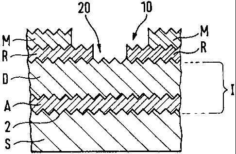
[0040] By way of example only, this is shown in figures 7 and 8 in a security
element with a layer structure according to figure 4. On the substrate S in
the form of a
plastic film with embossed diffraction structure 2 the interference element I
is vapor-
deposited and adjoining the interference element I at first the reflection
layer R and
then the magnetic layer M. The reflection layer R has gaps 20 in the form of a
repeated
writing "PL", as to be seen in figure 8. The gaps 10 in the magnetic layer M
are
substantially larger than the gaps 20 in the reflection layer R and form a
magnetic bar
code 11, as also to be seen in Fig. 8. The code can be seen, depending on the
embodiment, in the positive or negative patterns, i.e. in the magnetic areas
or in the
gaps.
[0041] Figure 8 shows an intermediate product 100 from top view for producing
numerous security elements 1 in the form of security threads 200 with the
cross-
section shown in figure 7. The gaps 20 in the form of the characters "PL" are
visible
through the interference element I and the transparent carrier material or
substrate S.
The magnetic layer M located behind the reflection layer R, and therefore not
visible
in plan view, is only present in partial areas 11 which form a bar code and
are faintly
marked in dot-and-dash pattern in figure 8.
[0042] The intermediate product 100 shown in figure 8, in a subsequent
procedure step, is separated along the separating line 101 so as to form
security threads
200 for the embedding in e.g. bank notes. The characters "PL" formed by the
gaps 20
in the reflection layer R are hardly discernible in incident light in a
security thread
embedded in a bank note, in transmitted light, however, they are perceptible
as
negative writing.
[0043] Security threads with a structure as described in figures 7 and 8 are
particularly suitable for the use as window security thread, which is embedded
in a
CA 02472353 2004-07-06
-11-
document in such a way, that it is at least in places directly visible or
emerging at the
surface. This is shown in figure 9 with the cross-section of a bank note 300
as
example. Methods for embedding the security thread 200 in paper under the
forming
of windows in the area of the security thread are described e.g. in DE-A-36 O1
114.
With a thread embedded in such a way, when viewed in incident light, in the
window
area mainly the diffraction structure or reflection pattern is visible,
however, when
viewed in transmitted light the negative writing present in the metal coating
dominates. In both cases the color shift effect caused by the interference
layer structure
remains perceptible.
[0044] The inventive security element thus combines in its simplest
embodiment three security features in an optimal way with each other, namely
on the
one hand a color shift effect in combination with an optimal reflecting metal
layer,
whose electrical conductivity forms a second security feature, and finally a
magnetic
security feature, whose properties can be optimally adjusted without
negatively
affecting the other security features.
[0045] Further security features can be combined with the inventive security
element, for example, by means of a partial removal of the reflection layer as
to form
patterns or symbols and/or partial removal of the magnetic layer as to form a
coding,
for example a bar code, as well as by combination with diffraction structures,
in
particular in the form of an embossed structure, preferably adjoining the
already
present reflection layer R.
[0046] One preferred area of use of the inventive security element has already
been stated above as security thread, in particular as machine-readable
magnetic-
hologram window security thread with color shift effect and negative writing.
However, the security element can also be bonded as stripe or plane element to
an
object, in particular a document of value, preferably a bank note, or in
another way
with or without the substrate be transferred to an object, for example by hot
stamping
method.