Note : Les descriptions sont présentées dans la langue officielle dans laquelle elles ont été soumises.
CA 02479384 2004-09-14
WO 03/087660 PCT/US03/10807
LIGHTING DEVICE AND METHOD
Background
1. Technical Field
[0001] The present invention relates generally to a lighting device including
a light emitting diode supported on an electrically insulated metal substrate.
2. Description of Prior Art
[0002] A light emitting diode (LED) includes a semiconductor chip that
emits light and heat in response to the application of an electrical current.
There
are two major types of LEDs, "packaged" and "unpackaged." A packaged LED is
one with a .solderable lead and a reflector cup. In a packaged LED, a
semiconductor chip, for example an Indium Gallium Nitride (InGaN) or Indium
Phosphide (InP) semiconductor chip, is housed in the reflector cup inside an
optically transparent epoxy shell.
[0003] An unpackaged LED is also available. An unpackaged LED has a
bare die, that is, the semiconductor chip has no solderable lead or reflective
cup.
Because an unpackaged LED lacks the solderable lead, an electrically
conductive
adhesive bonds the semiconductor chip directly to the circuit board. A wire
connects the top of the semiconductor chip to circuits on the circuit board.
The
wire is bonded to the circuit board after the semiconductor chip is bonded to
another conductive pad on the board.
[0004] Without a reflector cup, the unpackaged LED must rely on the
reflectivity of the surface of the circuit board. Coatings commonly used to
enhance the circuit board reflectivity can have long-term stability problems,
such
as diminished performance in high ultraviolet (UV) conditions, deterioration
due to
weathering, sensitivity to high temperatures, and age induced yellowing.
[0005] The unpackaged LED must also rely on the heat sinking ability of the
circuit board and the conductive adhesives used to bond the bare semiconductor
chip. Accordingly, the initial and long-term reflectivity of the board
surfaces, the
heat sinking ability of the circuit board material and the conductive
adhesive, and
1
CA 02479384 2004-09-14
WO 03/087660 PCT/US03/10807
the performance of the LED itself can define the LED performance level and
longevity.
[0006] A particular type of LED is a High Brightness LED (HBLED). The
HBLED emits an increased level of light in comparison to a conventional LED.
The HBLED has a longer useful life and consumes less power than a comparable
LED. Another type of LED is a semiconductor laser diode (LD).
[0007] In general, both the brightness of the light emitted and the amount of
heat generated increases as more electric current is applied to the LED. The
heat
shedding capacity of the LED defines an upper threshold for the application of
more current. Accordingly, the efficiency of the LED to shed heat limits the
brightness attainable by the LED.
[0008] To increase the total light output of a lighting device, multiple LEDs
or HBLEDs are combined to form an array. Such and array is called a light
engine. The light engine can contain from two to several thousands of LEDs.
The
more LEDs used, the larger the total light output from the light engine.
[0009] Light engines are generally manufactured using a fiberglass-epoxy
printed circuit board (PCB). Packaged LEDs are generally soldered onto the
circuit board. To increase the brightness of the illumination, the entire
circuit
board mounts on a heat sink device to remove the heat generated by the
operation of the LEDs. The heat sink device conducts heat away from the LEDs.
This can allow more current to be applied and, thus, more light to be emitted
by
the LEDs.
[0010] The PCB can also include resistors. The resistors can be printed
onto the PCB using organic or polymer based materials. Once on the PCB, the
resistors can be trimmed by, for example, a laser. This allows the resistors
to
attain very precise resistance tolerances. However, the heat from the trimming
operation can damage PCBs formed of traditional reinforced plastics. This
susceptibility to heat damage limits the usefulness of resistor trimming in
PCB
applications.
2
CA 02479384 2004-09-14
WO 03/087660 PCT/US03/10807
Summary
[0011] The present invention provides a new and improved apparatus for
use as a light emitting diode (LED) lighting device. The present invention
provides
a robust support for LEDs that affords excellent heat sink properties and the
ability
to laser trim circuitry without risk of damaging the underlying substrate. The
invention may include a high temperature coating layer having controlled
reflectance that offers long-term color stability and reflectivity. The
apparatus
includes a metal substrate having a surface with a dielectric coating layer
disposed on the surface of the metal substrate. A light emitting diode (LED)
is
supported on the dielectric coating layer. The metal substrate serves as a
heat
sink for the heat emitted by the LED during operation of the device.
(0012] The present invention also provides a method for making a light
emitting diode (LED) light engine. The method includes coating a metal
substrate
with a dielectric coating material. The method further includes mounting an
LED
on the coated metal substrate to form the light emitting diode (LED) light
engine.
[0013] The foregoing and other features of the invention are hereinafter
more fully described and particularly pointed out in the claims, the following
description setting forth in detail certain illustrative embodiments of the
invention,
these being indicative, however, of but a few of the various ways in which the
principles of the present invention may be employed.
Brief Description of the Drawings
(0014] Fig. 1 is a perspective schematic view of an apparatus comprising a
first embodiment of the invention;
[0015] Fig. 2 is a schematic cross-sectional view taken along line 2-2 in
Fig. 1;
[0016] Fig. 3 is a schematic perspective view of an apparatus comprising a
second embodiment of the invention;
(0017] Fig. 4 is a schematic cross-sectional view taken along line 4-4 in
Fig. 3;
[0018] Fig. 5 is a schematic cross-sectional view of part of an apparatus
comprising a third embodiment of the invention;
3
CA 02479384 2004-09-14
WO 03/087660 PCT/US03/10807
[0019] Fig. 6 is a schematic cross-sectional view of part of an apparatus
comprising a fourth embodiment of the invention; and
[0020] Figs. 7-8 are schematic cross-sectional views of additional
embodiments of the invention.
Detailed Description of Preferred Embodiments
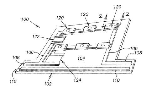
[0021] A light emitting apparatus 100 comprising a first embodiment of the
invention is shown in Fig. 1. The apparatus 100 is a lighting device including
light
emitting diodes (LEDs) on an electrically insulated metal substrate.
Specifically,
the apparatus 100 is an LED light engine for use in applications such as
signage
and lighting displays.
[0022] With reference to Figs. 1-2, the apparatus 100 includes a metal
substrate indicated generally by reference numeral 102. An inorganic porcelain
enamel layer 104 over-coats the metal substrate 102 to form an electrically
insulating dielectric layer. Electronic circuits 106 are arranged on the
enamel
layer 104. The electronic circuits 106 communicate first and second electronic
leads 108, 110 with a plurality of light emitting diodes 120. First and second
resistors 122, 124, in series with the LEDs 120, communicate with the first
electronic lead 108 through the circuits 106.
[0023] In this embodiment, the metal substrate 102 is low carbon
decarburized steel. The metal substrate 102 is prepared and coated with the
enamel layer 104 as described in U.S. Pat. Nos. 5,605,715 and 6,195,881
assigned to The Erie Ceramic Arts Company (Erie, PA), which are hereby
incorporated by reference in their entirety. Generally, an insulated steel
substrate
is formed by the process of forming a coupon of steel to the desired shape and
thickness, cleaning and/or pickling the steel. The steel is then immersed in a
conventional acidic copper sulphate solution after which it is dipped in a
slurry of
the desired coating material system such as a conventional electronic grade
porcelain enamel coating slurry. During the coating process the steel is
electrified
such that it acts as an anode and thus attracts the solid particles in the
slurry by
electrophoresis. When the coated steel is removed from the slurry, it is then
dried
4
CA 02479384 2004-09-14
WO 03/087660 PCT/US03/10807
and heated to a bonding temperature of around 1500°F in order to form
the
durable dielectric layer on the steel.
[0024] Metal substrates coated with a dielectric layer of electronic grade
porcelain enamel are commercially available under the trade name designation
ELPOR from the ECA Electronics Company (Erie, PA). Preferably, the dielectric
layer displays a leakage current of less than 50 ~, Amps at 350°C.
[0025] Any number of conventional dielectric or resistive coating materials
may be used in connection with the present invention. Such coatings may be
classified as either "porcelain enamel," "glass" or "ceramic" or
"glass/ceramic."
Such "porcelain enamel" or "glass" coatings may be referred to as "vitreous"
coatings. Such "ceramic" coatings may be referred to as "devitrified"
coatings.
[0026] Other suitable metal substrates coated with a dielectric layer and
their methods of production are disclosed in U.S. Patent No. 6,195,881 issued
to
Giardina et al; U.S. Patent No. 5,002,903 issued to Lim et al, U.S. Patent No.
4,361,654 issued to Ohmura et al; U.S. Patent No. 4,085,021 issued to Van der
Vliet; U.S. Patent No. 4,256,796 issued to Hang et al; U.S. Patent No.
4,358,541
issued to Andrus et al.; U.S. Patent No. 4,385,127 issued to Chyung; U.S.
Patent
No. 3,841,986 issued to Gazo et al.; and U.S. Patent No. 3,575,838 issued to
Hughes, which are hereby incorporated by reference in their entirety. It will
be
appreciated that whatever coating material system is employed, it must afford
good electrical properties and it must be competitive with commercially
available
thick film materials for use in forming the required circuit structure. As
used
herein, and the claims below, the term "insulating dielectric layer" is
intended to
encompass all of the above mentioned inorganic coating material systems.
[0027] The enamel layer 104 is an electronic grade porcelain enamel
coating that covers the entire top surface of the metal substrate 102. Over
the
enamel layer 104 are the conductive circuits 106. The enamel layer 104 being
disposed between the metal substrate 102 and the circuits 106, forms a
dielectric
layer between such substrate 102 and circuits 106.
[0028] The circuits 106 are thick film conductive circuits. Preferably, the
thick film is a silver cermet thick film. The silver cermet is generally
silver metal
particles in a boro-silicate glass matrix. Cermet thick films of various
formulations
CA 02479384 2004-09-14
WO 03/087660 PCT/US03/10807
for use in the present invention are commercially available from Electro-
Science
Laboratories, Inc. (King of Prussia, PA) and the Ferro Corporation of
Cleveland,
Ohio. The thick film circuits 106 are applied on top of the enamel layer 104
using
a conventional application technique. In this instance, the circuits 106
applied
using a screen-printing technique. In other embodiments, thick film circuits
may
be applied using other techniques involving, for example, direct writing,
spraying,
dipping, spinning, brushing or doctor blades. In yet another embodiment, a
thick
film circuit may be formed using a gold cermet thick film that is commercially
available from Electro-Science Laboratories, Inc. under the trade designation
8835.
[0029] As described above, the circuits 106 communicate the first and
second leads 108, 110 with various components supported on the apparatus 100.
The components include the resistors 122, 124 and the LEDs 120. The resistors
122, 124 are printed thick film resistors trimmed with lasers to attain
precise
resistances. Resistors may be formed using any one of a variety of cermet
thick
films also available from the Ferro Corporation or Electro-Science
Laboratories,
Inc. Laser trimming can increase uniformity of the resistors and cermet
materials
generally display a better service as compared to organic resistor materials
employed on prior art polymeric boards. Because the enamel layer 104 is
resistant to high temperatures, laser trimming of the resistors 122, 124 does
not
degrade the enamel layer 104 or the metal substrate 102.
(0030] The LEDs 120 are commercially available packaged high brightness
LEDs (HBLEDs). A commercially available conductive epoxy adhesive forms an
adhesive layer 130 to adhere the LED 120 to the circuit 106. In applications,
when the LED permits, conventional solder techniques may be employed to
mount the LED. The LED 120 includes a transparent plastic lens 132. The lens
132 can be a colored lens, if desired.
[0031] During operation, a forward electrical current is applied to the LEDs
120 through the circuits 106. The current is controlled by the resistors 122,
124.
In response to the electrical current, the LEDs 120 switch to ON and emit
light and
heat.
6
CA 02479384 2004-09-14
WO 03/087660 PCT/US03/10807
[0032] The surface of the enamel layer 104 reflects the emitted LED light
away from the surface. The metal substrate 102 serves as a heat sink and thus
it
conducts away the heat generated by the operating LEDs 120.
[0033] It will be appreciated that portions of the circuit 106 may be coated
with an encapsulated layer. A suitable encapsulant layer may be formed using a
glass encapsulant sold by the Ferro Corporation of Cleveland, Ohio, under the
trade designation A-3565. The glass encapsulant serves to prevent particulate
migration between individual circuit traces. The encapsulant may be applied,
for
example, by screen printing directly on the thick film materials and the top
surfaces of the dielectric layer and then the entire board may be fired at a
temperature of about 625°C.
[0034] With reference to Fig. 3, an apparatus 200 comprising a second
embodiment of the invention is shown. The apparatus 200 is an LED light engine
similar to the light engine of the apparatus 100. The light engine 200
includes a
metal substrate 202 comprising decarburized low carbon steel.
[0035] A porcelain enamel coating 204 forms a dielectric layer over the
surface of the metal substrate 202. A reflective inorganic enamel coating 206
forms a white reflective layer superimposed over the enamel coating layer 205.
In
applications where the reflectivity of light is desired, a white coating is
employed.
Preferably, the white coating displays a reflectivity of at least 80%. Various
white
enamel coating material systems are commercially available from companies such
as the Ferro Glass & Color Corporation of Washington, Pennsylvania. Applicants
believe that an enamel having high reflectivity is best achieved by the
formulation
of a ball milled enamel powder comprising by weight 1000 parts 14390 glass
frit
available from Chi-Vit of Urbana, Ohio, 60 parts anatase titanium dioxide, 15
parts
syloid colloidal silica available from W. R. Grace, 13 parts cerium oxide, 1.3
parts
potassium nitrate, 0.6 parts potassium chloride and 3.8 parts 5500 colloidal
alumina available from the Ferro Corporation. The powder is then mixed with a
suitable carrier such as pine oil to facilitate screen printing or other
application
techniques. The enamel layer may be applied using conventional techniques
upon the dielectric layer during the application of the circuit traces, and
fired along
with the circuit trace materials.
7
CA 02479384 2004-09-14
WO 03/087660 PCT/US03/10807
[0036] First and second thick film circuits 220, 222 are formed on the
enamel coating 204 using methods known to one skilled in the art. First and
second electrical leads 224, 226 communicate with a thermal sensor
(thermistor)
228 through the first circuit 220. Third and fourth electrical leads 230, 232
communicate with an of unpackaged or bare die array of LEDs 234 through the
second circuit 222.
[0037] The first and second circuits 220, 222 are in part disposed between
the enamel coating 204 and the reflective coating 206. The reflective coating
206
is arranged over the first and second circuits 220, 222,but under the array
234 and
the thermal sensor 228. However, the electrical leads 224, 226, 232, 234 each
have portions that are not covered by the reflective coating 206. The
reflective
coating 206 is positioned both to reflect a portion of the emitted light from
the
array 234 away from the light engine 200, and to allow electrical contact with
portions of the electrical leads 224, 226, 232, 234.
[0038] With reference to Fig. 4, a cross sectional view of a portion of the
light engine 200 is shown. The ceramic coating layer 204 is disposed between
the electrical leads 224, 226, 232, 234 and the metal substrate 202. In
contrast,
the reflective coating 206 covers portions of the electrical leads 224, 226,
232,
234 but is not located between the electrical leads 224, 226, 232, 234 and the
metal substrate 202.
[0039] During operation, a forward electrical current is applied to the leads
224, 226, 232, 234 and through the first circuit 220 to the thermal sensor
228, and
through the second circuit 222 to the array of LEDs 234.
[0040] In response to the electrical current, the array of LEDs 234 emit light
and heat. The reflective coating 206 reflects light away from its surface and
the
metal substrate 202 conducts away heat generated by the operating array of
LEDs 234.
[0041] The thermal sensor 228 senses the temperature of the substrate
202 and the ambient air. The sensor 228 then signals a controller (not shown)
that can adjust the current application to the array of LEDs 234 in response
to the
signal.
8
CA 02479384 2004-09-14
WO 03/087660 PCT/US03/10807
[0042] In Fig. 5, an apparatus 300 comprising a third embodiment of the
invention is shown. The apparatus 300 includes a decarburized steel substrate
302. An electrically insulative dielectric layer 304 coats the metal substrate
302.
Superimposed on a portion of the coating layer 304 is an inorganic white layer
306. However, it will be appreciated that any number of colored (controlled
reflectance) enamels, such as black enamel, may be employed depending upon
the desired reflectivity properties. High temperature enamels in various
colors are
available from the Ferro Corporation.
[0043] A plurality of unpackaged LEDs each include a gold wire 310 and an
InGaN semiconductor chip 314. The chip 314 is adhered by an adhesive layer
316 to a first thick film, conductive printed circuit 318. The wire
communicates
with a second thick film, conductive printed circuit 320.
[0044] During operation, a negative (-) electrical potential is applied to the
first circuit 318 and a positive (+) electric potential is applied to the
second circuit
320. The chip 314 communicates with the first and second circuits 318, 320
through the conductive adhesive 316 and through the wire 312, respectively.
The
chip 314 responds to the application of the electric potential by emitting
light and
heat. The white layer 306 reflects the light contacting the white layer 306.
The
metal substrate 302 conducts heat away from the chip 314.
[0045] With reference to Fig. 6, a cross-sectional view of part of an
apparatus 400 comprising a fourth embodiment of the invention is shown. The
apparatus 400 is a light engine including a stainless steel substrate 402. The
stainless steel substrate 402 is overcoated with an electronic grade porcelain
enamel coating layer 404.
[0046] Superimposed over the coating layer 404 is a plurality of dielectric
coating layers. Specifically, first, second and third layers 410, 412, 414 of
dielectric material cover a portion of the surface of the coating layer 404.
Separated from each other by interspersion between the dielectric layers are a
plurality of thick film conductors. Specifically, first, second and third
conductors
420, 422, 424 are separated from each other by the first, second and third
dielectric layers 410, 412, 414, respectively.
9
CA 02479384 2004-09-14
WO 03/087660 PCT/US03/10807
[0047] Dielectric layers 410, 412 and 414 are produced by forming a
dielectric coating using multiple discrete homogeneous layers of commercially
available thick film dielectric materials intended for use on metal
substrates.
Examples of such materials include a thick film material available from
Electro-
Science Laboratories, Inc. of King of Prussia, Pennsylvania, under the trade
designation 4924, thick film materials available from DuPont of Wilmington,
Delaware, under the trade designation 3500N and thick film materials available
from Heraeus of West Conshohocken, Pennsylvania, under the trade designation
IP-222. These materials are intended for use in making thick film heaters, but
applicants have unexpectedly found them suitable for use in the present
invention.
[0048] The thick film dielectric materials are applied in multiple layers upon
the enamel layer 404 and then they are fired at a temperature of about
850°C.
The layers are preferably applied by screen printing and have a thickness of
about
.006" after firing. However, other application techniques such as spraying
could
be utilized. Each applied layer is dried prior to application of the
subsequent
layer. It will be appreciated that dielectric layers 410, 412 and 414 may be
formed
directly upon the stainless steel substrate 402. Prior to application of the
dielectric
materials the stainless steel surface is thoroughly cleaned, and preferably
the
stainless grade employed is grade 430.
[0049] A plurality of unpackaged LEDs are supported on the apparatus 400.
A first LED 430 communicates with the first conductor 420, a second LED 432
communicates with the second conductor 422, and a third LED 434
communicates with the third conductor 424. Specifically, the LEDs 430, 432,
434
each communicate with the conductors 420, 422, 424 through conductive
structures called vias 440, 442, 444, respectively. The LEDs 430, 432, 434
include
semiconductor chips 446, 448, 450 that communicate through conductive wire
leads 452, 454, 456 with thick film resistor circuits 460, 462, 464,
respectively.
[0050] The LEDs 430, 432, 434 are different colors from each other.
Specifically, the LED 430 emits a red light, the LED 432 emits a blue light,
and the
LED 434 emits a yellow light in response to an application of an electric
current.
[0051] During operation, an electric current is applied to the circuits 460,
462, 464. In response to the electric current, the LEDs 430, 432, 434 emit
light
CA 02479384 2004-09-14
WO 03/087660 PCT/US03/10807
and heat. Because the circuits 460, 462, 464 are electrically independent of
each
other, the application of the electric current can be separately controlled to
each of
the LEDs 430, 432, 434. Accordingly, the LEDs 430, 432, 434 can be separately
controlled to switch ON and OFF.
[0052] When the LEDs 430, 432, 434 are switched ON, the heat that they
generate is conducted away through the stainless steel substrate 402.
[0053] It will be appreciated that multilayer structures may also be formed
by taking a porcelain enamel metal coated substrate available from ECA
Electronics Company under the trade designation ELPOR and coating it with a
high performance electronic grade porcelain enamel coating material available
from the Ferro Corporation of Cleveland, Ohio, under the trade designation QP-
330. The ECA substrate with its enamel coating provides a bottom or first
dielectric layer, and the QP-330 provides top second layer. QP-330 may be
applied wet to the ECA porcelain coated substrates and then fired at about
800°C.
The QP-330 material may either be applied by dipping or screen printing to a
thickness of about .002" (after firing). One or more layers of the QP-330
material
may be applied successfully to the ECA porcelain coated substrates.
[0054] With reference to Fig. 7, an apparatus 500 comprising a fifth
embodiment of the invention is shown. The apparatus 500 is a metal core
circuit
board supporting LEDs. The apparatus 500 includes a decarburized steel
substrate 502. A reflective coating 504 is superimposed on an upper surface of
the substrate 502 and a conductive thick film circuit pattern 506 is
superimposed
on a lower surface of the substrate 502.
[0055] An array of apertures 510 extends from the upper side to the lower
side through the substrate 502. The array 510 is arranged such that pairs of
closely spaced apertures are spaced apart from other pairs of closely spaced
apertures.
[0056] Mounted on the upper side of the substrate 502 is a plurality of
leaded or line-terminated, packaged LEDs 512. The LEDs 512 each have a pair
of solderable leads 514 that extend through one of the pairs of closely spaced
apertures. The leads 514 are soldered to the circuit pattern 506 on the under
side
11
CA 02479384 2004-09-14
WO 03/087660 PCT/US03/10807
of the substrate 502 to secure the LEDs 512 to the upper side of the substrate
502.
[0057] Fig. 8 shows an apparatus 600 comprising another embodiment of
the invention. The apparatus 600 includes many parts that are substantially
the
same as parts of the apparatus 500; this is indicated by the use of the same
reference numerals in Figs. 7 and 8. The apparatus 600 differs from the
apparatus 500 in that the apparatus 600 includes an array of apertures 602
sized
and shaped to accommodate the insertion of a corresponding plurality of
packaged LEDs 604.
[0058] The LEDs 604 are mounted to the lower side of the substrate 502,
but partially extend through the array of apertures 602 to the upper side. The
leads 514 are soldered or bonded with a conductive epoxy to the circuit
pattern
506 to secure the LEDs 604 to the substrate 502.
(0059] During operation, an electric current is applied to the circuit pattern
506 and subsequently to the leads 514. In response to the electric current,
the
LEDs 512, 604 emit light and heat. Heat is conducted away from the LEDs 512,
514 by the substrate 502.
[0060] Also envisioned are alternative embodiments which have substrates
comprising metals that differ from the metals disclosed above. Such substrates
may comprise, for example, a ferrous alloy such as a carbon-steel or another
metal, such as copper, aluminum and copper-beryllium.
(0061] The embodiments described herein are examples of structures
having elements corresponding to the elements of the invention recited in the
claims. This written description may enable those skilled in the art to make
and
use embodiments having alternative elements that likewise correspond to the
elements of the invention recited in the claims. The intended scope of the
invention thus includes other structures that do not differ from the literal
language
of the claims, and further includes other structures, systems or methods with
insubstantial differences from the literal language of the claims.
12