Sélection de la langue

Search

Sommaire du brevet 2536994 

Énoncé de désistement de responsabilité concernant l'information provenant de tiers

Une partie des informations de ce site Web a été fournie par des sources externes. Le gouvernement du Canada n'assume aucune responsabilité concernant la précision, l'actualité ou la fiabilité des informations fournies par les sources externes. Les utilisateurs qui désirent employer cette information devraient consulter directement la source des informations. Le contenu fourni par les sources externes n'est pas assujetti aux exigences sur les langues officielles, la protection des renseignements personnels et l'accessibilité.

Disponibilité de l'Abrégé et des Revendications

L'apparition de différences dans le texte et l'image des Revendications et de l'Abrégé dépend du moment auquel le document est publié. Les textes des Revendications et de l'Abrégé sont affichés :

  • lorsque la demande peut être examinée par le public;
  • lorsque le brevet est émis (délivrance).
(12) Demande de brevet: (11) CA 2536994
(54) Titre français: GESTION DE BLOCS DEFECTUEUX DANS DES MEMOIRES FLASH
(54) Titre anglais: MANAGEMENT OF DEFECTIVE BLOCKS IN FLASH MEMORIES
Statut: Morte
Données bibliographiques
Abrégés

Abrégé français

L'invention concerne un procédé de gestion de blocs mémoire défectueux dans un système à mémoire non volatile, comprenant des blocs mémoire (SB) effaçables individuellement, adressables au moyen d'adresses de blocs mémoire réelles (SBA), lesdits blocs mémoire étant adressables au moyen d'une conversion d'adresse utilisant une table d'affectation (ZT) pour convertir des adresses de blocs logiques (LBA) en l'une des adresses de blocs mémoire réelles respectives (SBA). La table d'affectation (ZT) est subdivisée en au moins une zone de données utiles (NB), une zone à bloc tampon (BB), une zone de défauts (DB) et une zone de réserve (RB). L'invention est caractérisée en ce que, lorsqu'une erreur se produit lors de l'effaçage, le bloc correspondant est remplacé par un bloc de réserve et son adresse de bloc mémoire est introduite dans la zone de défauts (DB).


Abrégé anglais


The invention relates to a method for the management of defective memory
blocks in a non-volatile memory system comprising individually erasable memory
blocks (SB) that can be addressed with the aid of real memory block addresses
(SBA). Said memory blocks can be addressed by means of an address conversion
that uses an allocator table (ZT) to convert logical block addresses (LBA)
into one of the respective memory block addresses (SBA). According to the
invention, the allocator table (ZT) is sub-divided into at least one useful
data area (NB), a buffer block area (BB), a defect area (DB) and a reserve
area (RB). If an error occurs during the erasure process, the relevant block
is replaced by a reserve block and its memory block address is written to the
defect area (DB).

Revendications

Note : Les revendications sont présentées dans la langue officielle dans laquelle elles ont été soumises.


-4-


Claims

1. Method for the management of defective memory blocks in a non volatile
memory system
with individually erasable memory blocks (5B), addressable with real memory
block
addresses (SBA), and which arc addressable with an address conversion by means
of a
allocator table (ZT) of logical block addresses (LBA) into one of the real
memory block.
addresses (SBA), characterized in that the allocator table (ZT) is divided
into a useful data
area (NB), a buffer block area (BB), a defect area (DB) and a reserve area
(RB), and that after
an error with the erasure of a block the allocator table (ZT) is changed in
that way that the
memory block address of the corresponding memory block is registered into the
defect area
(RbB) and at its place a block is addressed, which was previously registered
in the reserve area
2. Method according to claim 1, by the fact characterized that the defect area
(DB) contains
in each case so much entries, as defective blocks are present.
3. Method according to claim 2, characterized in that the defect area (DB) is
increased by
one entry on registering a defective block and the reserve area (RB) is
reduced by one entry.
4. Method according to claim 3, characterized in that the quality of the
memory is determined
by the relationship of the number of the entries of the reserve area (RB) to
the defect area
(DB).
5. Method according to claim 1, characterized in that after errors during the
write operation
into a memory block (SB) the corresponding block is marked by the flag
"defect" (DEF).
6. Method according to claim 5, characterized in that a background program
scans the
allocator table (ZT) for memory blocks (SB), which can be erased, and does
erase these, but if
such a memory block is marked With the flag "defect", does not erase this, but
registers it into
the defect area (DB).

Description

Note : Les descriptions sont présentées dans la langue officielle dans laquelle elles ont été soumises.


CA 02536994 2006-02-24
Our Ref: ~1 ~ 59-2U k~10 20051027 3 39 Al
_1_
Managexx~ent of defective blocks in flash memory
The invention is related to a method to manage defective memory blocks in a
noxz-volatile
memory system comprising individually erasable memory blocks, that can be
addresses with
the aid of real memory block addresses Said memory block addresses can be
addressed by
means of an address conversion that uses an allocator table to convert logical
block addresses
into one of the respective memory block addresses. The allacator table is sub-
divided into at
least one useful data area, a buffer block area, a defect area and a reserve
area_
Flash memories are used in many computer systems, in particular iz~ changeable
memory
cards for digital cameras and portable computers. Flash memories are organised
in memory
blocks, each with a lot of sectors. The limited number of write and erase
operations and the
erasure of only large memory blocks are essential features of these memories.
Thereby the
write and erase operations need much more time (up to a factor of 50) as the
read operation.
The memory blocks are weaned out through many write and erase operations and
then they are
no longer reliable at writing and erasure.
Through wear levelling, as described in 1_e_ in the patent application DL 198
40 359, an
approximately equal number of erase operations is achiewed_ As through modern
production
technology the quality and with it the frequency of erase operations are
szm~ilar for all memory
cells, management methods can be used, which are equal fvr all memory blocks.
With lsan~owr~ methods, 1_e_ with the patent application EP 0,617,353, by
recognition of a defect:
block this will be substituted by a reserve block and these two are chained in
a table.
Furthermore, a table on defect mezxaory cells is maintained. Such methods tend
to a longer
seek in tables to find the valid memory block to a memory operation.
It is the task of the invention to manage defective memory blocks in such a
way, that they are
r~o longer included in memory operations.
This task is solved in that if an error occurs during an erase process the
relevant block is
replaced by a reserve block and its memory block address is written into the
defect area.


CA 02536994 2006-02-24
-2-
Favourable embodiments of the invention are specified in the dependent claims.
The considered memory systenn with non-volatile memory cells is organised in
memory
blocks, which are individually erasable with an erasure operation,
lie memory blocks are addressed by their memory block address. The logical
block
addz-esses, given by a host system, are converted into memory block addresses
by means of an
allocator table_ Thereby the logical block addresses are allocated in
continuous order. The
logical block address serves as index into the allocator table, in which to
each logical address
a memory block address is reb stered, which in use can be exchanged with other
metx~ory
block addresses. Xn addition for each memory block flags are maintained in the
table.
The allocator table is divided into at least four areas: a useful data area, a
bui~'er block area, a
reserve area and a defect area, which attach directly together. The useful
data area is the by
far largest area. Far a memory system with 1000 memory blocks division could
be for
example arranged as follows: 9~4 useful data blocks, 4 buffer blocks, first S2
reserve blocks
and 2 defect blocks_ On occurrence of an error at an erasure operation, the
entry ofthe
memory block in the allocator table is exchanged with a reserve block and its
address is
registered into the defect area.
Favourable the defect area is in each case only so large, as defective blocks
have been
registered. If a new defective block is recognized, the defect area is
increased by an entry and
the reserve area is reduced by an entry. The total volume of the reserve area
plus the defect
area does remain constant and there are no further table changes necessary.
Since all memory cells have about the same probability of defeat, and
favourable the erase
frequency is adapted through "wear levelling" of all memory blocks, the
relationship between
defective and reserve blocks indicates the quality and the total wear of the
memory system,
which can be simply evaluated.
rf an error is recognized during the writing into a memory block, it is marked
by the flag
"defect". Since only few bits arc wrong with such an error, the bit errors are
corrected by
means of the check bytes during the reading ofthis block and the correct
contents is
reproduced. Only before the next writing to the as "defect" characterized
memory block this
is exchanged with another memory block from the buffer area_
The erasure of used and no longer valid memory blocks is favourable done by a
background
program, which evaluates appropriate flags to the memory blocks_ lfthis
program detects a

CA 02536994 2006-02-24
-3-
memory block characterized with the flag "is defect", this is not erased, but
is directly
exchanged with a reserve block. Zn the future the defective block is not any
longer used.
A favourable embodiment of the invention is described exemplaril~y in the fi~
res.
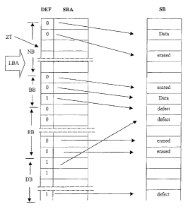
Pig_ 1 shows the structure of the allocator table to the memory blocks at the
occurrence of a
defect.
Fig. 2 shows the allocator table after clearing due to a write error
In Fig. 1 the alloeator table time is represented, which is divided into four
areas_ The first
area is the useful data area NB, which takes the by far largest part of the
table_ Then the
bufTer block area BB with some pointers to buffer blocks. The reserve area
contains pointers
to erase blocks, which stand ready as spare. The defect area points only to
defective blocks.
The allocator table is accessed with a logical block address LBA and then the
there registered
memory block address SBA is used for the xnen~ory operation. The memory blocks
SB can
contain data, caz~ be erased ("erased") or defective("defect")_ Write
operations to a memory
block SB use normally a bufFer block. Tf during the write operation it is
recog i7ed that the
memory block is defective, the flag DBF is set amd a new buffer block from the
reserve area is
used.
In Fig. 2 the situation of the allocator table time is shown after clearing of
the write error. The
buffer block pointer, which pointed first to a defective memory block SB,
points now to an
erased memory 'block, which was assigned so far to the reserve area RB. The
reserve area RB
is reduced by one entry and the defect area DB is enlarged by one entry. The
border between
both areas is shifted by one entry. The total sum of the assigned blocks to
the two areas
remained constant.

Dessin représentatif
Une figure unique qui représente un dessin illustrant l'invention.
États administratifs

Pour une meilleure compréhension de l'état de la demande ou brevet qui figure sur cette page, la rubrique Mise en garde , et les descriptions de Brevet , États administratifs , Taxes périodiques et Historique des paiements devraient être consultées.

États administratifs

Titre Date
Date de délivrance prévu Non disponible
(86) Date de dépôt PCT 2004-08-12
(87) Date de publication PCT 2005-03-24
(85) Entrée nationale 2006-02-24
Requête d'examen 2008-08-15
Demande morte 2010-08-12

Historique d'abandonnement

Date d'abandonnement Raison Reinstatement Date
2009-08-12 Taxe périodique sur la demande impayée

Historique des paiements

Type de taxes Anniversaire Échéance Montant payé Date payée
Enregistrement de documents 100,00 $ 2006-02-24
Le dépôt d'une demande de brevet 400,00 $ 2006-02-24
Taxe de maintien en état - Demande - nouvelle loi 2 2006-08-14 100,00 $ 2006-08-09
Taxe de maintien en état - Demande - nouvelle loi 3 2007-08-13 100,00 $ 2007-08-09
Taxe de maintien en état - Demande - nouvelle loi 4 2008-08-12 100,00 $ 2008-07-23
Requête d'examen 800,00 $ 2008-08-15
Titulaires au dossier

Les titulaires actuels et antérieures au dossier sont affichés en ordre alphabétique.

Titulaires actuels au dossier
HYPERSTONE AG
Titulaires antérieures au dossier
KUEHNE, REINHARD
Les propriétaires antérieurs qui ne figurent pas dans la liste des « Propriétaires au dossier » apparaîtront dans d'autres documents au dossier.
Documents

Pour visionner les fichiers sélectionnés, entrer le code reCAPTCHA :


Pour visualiser une image, cliquer sur un lien dans la colonne description du document. Pour télécharger l'image (les images), cliquer l'une ou plusieurs cases à cocher dans la première colonne et ensuite cliquer sur le bouton "Télécharger sélection en format PDF (archive Zip)" ou le bouton "Télécharger sélection (en un fichier PDF fusionné)".

Liste des documents de brevet publiés et non publiés sur la BDBC .

Si vous avez des difficultés à accéder au contenu, veuillez communiquer avec le Centre de services à la clientèle au 1-866-997-1936, ou envoyer un courriel au Centre de service à la clientèle de l'OPIC.


Description du
Document 
Date
(yyyy-mm-dd) 
Nombre de pages   Taille de l'image (Ko) 
Abrégé 2006-02-24 1 19
Revendications 2006-02-24 1 41
Dessins 2006-02-24 2 30
Description 2006-02-24 3 146
Dessins représentatifs 2006-05-01 1 8
Page couverture 2006-05-02 2 45
PCT 2006-02-24 4 152
Cession 2006-02-24 4 97
Correspondance 2006-04-28 1 26
Cession 2006-05-25 2 59
Poursuite-Amendment 2008-08-15 1 40