Note : Les descriptions sont présentées dans la langue officielle dans laquelle elles ont été soumises.
CA 02547029 2006-05-19
EXPRESS MAIL NO. EV484958713US
Docket No. 59259-69WO
COMPENSATION SYSTEM AND METHOD FOR NEGATIVE CAPACITIVE COUPLING IN IDC
BACKGROUND OF THE INVENTION
Field of the Invention
The present invention is directed to communication connectors, and, more
specifically, to a communication connector with improved crosstalk reduction.
Description of the Related Art
The widespread use of communication devices has spurred the
development of communication connectors. Initially, communication devices such
as
telephones, computer terminals, and the like were hardwired. For example, the
wire
cable for a telephone was coupled directly through a hole in a wall plate to
electrical
terminals.
Modern telephone connectors use an industry standard receptacle
mounted in the wall and a mating industry standard plug at the end of a
telephone cord.
The use of industry standard connectors permits the convenient installation of
telephones. Similarly, industry standard connectors have been developed for
other
communication devices such as computers. For example, a personal computer may
be
coupled to a local area network (LAN) via a communication connector similar to
those
used with telephones.
The use of communication connectors with telephones does not result in
the degradation of signal quality because telephones typically have limited
bandwidth.
However, high-speed communication devices, such as computers, can suffer
significant
degradation of signal quality due to conditions such as crosstalk occurring
where a
signal on a line pair interferes with a signal on another line pair.
Conventional insulation displacement connector (IDC) designs have
associated capacitive and inductive crosstalk that hinders efforts to comply
with
sophisticated communication standards. Past attempts to satisfy Category 6
communication standards have sought to reduce the detrimental effects
potentially
caused by IDCs through use of configurations for the IDC different than the
configurations for the conventional IDCs. Having different IDC configurations
can be
undesirable, however, since other problems can be introduced including those
involved
with equipment logistics and support.
1
CA 02547029 2006-05-19
WO 2005/053324 PCT/US2004/039377
BRIEF SUMMARY OF THE INVENTION
The present invention resides in a patch panel crosstalk reduction system
and method. Aspects are for a at least one plug connector, the plug connector
having a
plurality of plug connector elements being grouped into pairs, including first
and second
pairs, each pair of the plurality of plug connector elements having a tip plug
connector
element and a ring plug connector element configured to be coupled to a
different wire
pair. Aspects include a jack connector shaped to receive the plug connector.
The jack
connector has a plurality of jack contact members and is configured to receive
the plug
connector such that each of the plurality of jack contact members is
electrically coupled
to a different one of the plurality of plug connector elements. The plurality
of jack
contact members includes a first tip jack contact member and a first ring jack
contact
member positioned to electrically couple with the tip plug connector element
and the
ring plug connector element, respectively, of the first pair of the plurality
of plug
connector elements when the jack connector receives the plug connector, and a
second tip jack contact member and a second ring jack contact member
positioned to
electrically couple with the tip plug connector element and the ring plug
connector
element, respectively, of the second pair of plug connector elements when the
jack
connector receives the plug connector.
An insulation displacement connector (IDC) is configured to receive a
plurality of wires and have a plurality of IDC elements, each of the plurality
of IDC
elements is configured to be coupled to a different one of the plurality of
wires. The
plurality of IDC elements is grouped into pairs. Each pair of the plurality of
IDC
elements has a tip IDC element and a ring IDC element configured to be coupled
to a
different wire pair. A first pair of IDC elements has a first tip IDC element
and a first
ring IDC element. A second pair of IDC elements has a second tip IDC element
and a
second ring IDC element. The first ring IDC element and the second tip IDC
element
are adjacent to each other and have a first capacitance therebetween.
A circuit board has a plurality of jack pads, a plurality of IDC pads, and a
plurality of internal conductors. Each of the plurality of jack pads are
electrically
coupled to a different one of the plurality of jack contact members so that a
first tip jack
pad, a first ring jack pad, a second tip jack pad, and a second ring jack pad
are
electrically coupled to the first tip jack contact member, the first ring jack
contact
member, the second tip jack contact member, and the second ring jack contact
member, respectively. Each of the plurality of IDC pads are electrically
coupled to a
2
CA 02547029 2006-05-19
WO 2005/053324 PCT/US2004/039377
different one of the plurality of IDC elements. Each of the plurality of
internal
conductors are electrically coupled to a different one of the plurality of
jack pads and a
different one of the plurality of IDC pads. The circuit board has a first
interdigitated
capacitance electrically coupled to the first tip IDC element and electrically
coupled to
the second tip IDC element and has a second interdigitated capacitance
electrically
coupled to the first ring IDC element and electrically coupled to the second
ring IDC
element. The first interdigitated capacitance and the second interdigitated
capacitance
is sized to reduce crosstalk associated with the first capacitance.
Other features and advantages of the invention will become apparent
from the following detailed description, taken in conjunction with the
accompanying
drawings.
BRIEF DESCRIPTION OF THE SEVERAL VIEWS OF THE DRAWING(S)
Figure 1A is a schematic diagram illustrating a conventional
communication transmission system.
Figure 1 B is a schematic diagram illustrating a conventional technique for
transmission of communication signals using differential circuitry and a
twisted pair wire
cable.
Figure 2A is a schematic diagram of a conventional plug connector for
use with the twisted pair wire cable of Figure 1 B.
Figure 2B is a perspective view of plug connector elements of the
conventional plug connector of Figure 2A.
Figure 2C is a front schematic view of the conventional plug connector of
Figure 2A showing pin assignment and configuration of the plug connector
elements.
Figure 2D is a top schematic sectional view of the conventional plug
connector of Figure 2A showing the wire pairs associated with the plug
connector
elements shown in Figure 2C.
Figure 2E is an isometric sectional view of the conventional plug
connector and associated conventional mating communication jack connector.
Figure 3 is an isometric view of a reduced crosstalk patch panel of the
present invention.
Figure 4 is an isometric view of the reverse side of the patch panel of
Figure 3.
Figure 5 is an electrical schematic of a first exemplary implementation of
3
CA 02547029 2006-05-19
WO 2005/053324 PCT/US2004/039377
the patch panel of Figure 3.
Figure 6 is a schematic diagram showing an exemplary lamination
sequence for the circuit board of the patch panel of Figure 3.
Figure 7 is a schematic diagram showing the first wire trace layer of the
lamination sequence of Figure 6.
Figure 8 is a schematic diagram showing the second wire trace layer of
the lamination sequence of Figure 6.
Figure 9 is a schematic diagram showing the third wire trace layer for the
lamination sequence of Figure 6.
Figure 10 is a schematic diagram showing the fourth wire trace layer for
the lamination sequence of Figure 6.
DETAILED DESCRIPTION OF THE INVENTION
A patch panel with crosstalk reduction system and method is described
herein to meet category 6 requirements while allowing for physical connector
configurations that are compatible with other standards such as category 5 and
category 5e. The development of a category 6 component compliant patch panel
per
TIA-568-B.2-1 standards for near-end crosstalk (NEXT) includes addressing
crosstalk
created in the associated RJ-45 plug and applying cancellation techniques in a
jack
position of a patch panel module so that the NEXT of the connector satisfies
the
specification. Conventional IDCs introduce a certain amount of crosstalk that
must be
dealt with in addition to the crosstalk created in the RJ-45 plug.
Conventional category
6 designs reduce the impact of the IDC by changing the IDC to a non-standard
configuration. For instance, in some conventional approaches, the spacing
between
pairs of IDC contacts are increased, which minimizes the capacitive crosstalk.
In these
approaches, the space between individual contacts in a pair is also decreased,
which
along with the larger spacing between pairs, decreases inductive crosstalk.
The present patch panel system with crosstalk reduction system and
method uses an approach to reduce the impact of the IDC to meet category 6
requirements so that these configuration changes of conventional approaches do
not
have to be used. In particular, for some of the present implementations, IDC
contact
spacing is 0.150 inches with a spacing tolerance of plus or minus 0.005
inches, which is
an industry standard spacing used for IDCs such as with category 5 compliant
IDCs
and other IDCs. With this industry standard spacing, these present
implementations of
4
CA 02547029 2006-05-19
WO 2005/053324 PCT/US2004/039377
IDCS are able to meet present Category 6 requirements (TIA 568-B.2-1
Commercial
Building Telecommunications Cabling Standard, Part 2: Balanced Twisted-Pair
Cabling
Components, Addendum 1: Transmission Performance Specifications for 4-Pair
Category 6 Cabling) for Near End Cross Talk (NEXT). In particular, to pass
this
Category 6 specification, NEXT of a system having a plug connector 40
(described
below, see Figure 2A) coupled with a patch panel 100 (described below, see
Figure 3)
must be less than (more negative) or equal to a NEXT limit line for
frequencies from 1
to 250 MHz described by the following NEXT limit line equation:
NEXT limit line (dB) = -(54 - 20*log(f/100)) wherein f represents frequency
in MHz for the range of f from 1 to 250 MHz and wherein for any first
frequency
between 1 to 250 MHz where the NEXT limit line equation yields a result that
is less
than -75dB, the Next limit line for the first frequency is equal to -75dB.
As described further below, steps are taken to directly address those pin
pairs that are most influenced by the capacitive properties of the IDC.
Communication connectors offer easy and reliable connections for a
variety of communication devices. A conventional communication transmission
system
is illustrated in the schematic diagram of Figure IA. The transmission system
includes
line drivers 2 and 4 and corresponding line receivers 6 and 8. A wire
conductor 10
connects the line driver 2 to the line receiver 6. A wire conductor 12
connects the line
driver 4 to the line receiver 8. Figure 1A illustrates the wire conductors 10
and 12 as
single conductors, which are typically bundled together as portions of a cable
14.
The wire conductors 10 and 12 are generally twisted in a parallel fashion
to each other for the length of the cable 14. A capacitance CDIST and
inductance
LDIST are shown in Figure 1A to model a distributed capacitive and inductive
coupling
between the wire conductors 10 and 12. A mutual inductance between the two
inductances LDIST and the capacitance CDIST contributes to the coupling of
electrical
signals between the wire conductors 10 and 12. The signal that is coupled
capacitively
or inductively between conductors is an undesirable signal that may be termed
a
"leakage" signal or "crosstalk." At low frequencies, such as are typical in a
telephone,
the crosstalk between the wire conductors 10 and 12 is minimal because the
distributed
capacitance CDIST and inductance LDIST provide low coupling at such low
frequencies. However, at higher frequencies, the crosstalk between the wire
conductors 10 and 12 becomes significant.
To minimize crosstalk, designers often use twisted pair cables and
5
CA 02547029 2006-05-19
WO 2005/053324 PCT/US2004/039377
differential amplifiers, such as illustrated in Figure 1 B. Figure 1 B
includes differential
line drivers 18, 20, 21 and 22, which are coupled to differential line
receivers 24, 26, 27
and 28, respectively. The differential line driver 18 is coupled to the
differential line
receiver 24 by a twisted pair cable 30 having a "tip" wire 30a and a "ring"
wire 30b.
Similarly, a twisted pair cable 32, having a "tip" wire 32a and a "ring" wire
32b, couples
the differential line driver 20 to the differential line receiver 26, a
twisted pair cable 34
having a "tip" wire 34a and a "ring" wire 34b couples the differential line
driver 21 to the
differential line receiver 27, and a twisted pair cable 36 having a "tip" wire
36a and a
"ring" wire 36b couples the differential line driver 22 to the differential
line receiver 28.
The twisted pair cables 30-36 are typically referred to as twisted wire pairs
or wire pairs
(possibly not all portions being twisted) and are portions of a cable 38. Each
of the
twisted pair cables 30-36 may be individually shielded to provide additional
protection
from crosstalk.
As is known in the art, the differential line receivers 24-28 are designed to
reject signals that are present on both conductors of their respective twisted
pair
cables 30-36. The degree to which the differential line receivers 24-28 can
reject these
"common mode" signals is indicated by a common mode rejection ratio (CMRR).
The
system illustrated in Figure 1 B is an improvement over that illustrated in
Figure 1A
because crosstalk between the twisted pair cables is canceled out by the CMRR
of the
differential line receivers. For example, a signal transmitted over the
twisted pair
cable 34 may be capacitively and inductively coupled to the twisted pair cable
30.
However, the capacitive coupling between the "tip" wire 34a and the "ring"
wire 34b
associated with the twisted pair cable 34 is substantially equal to the
capacitive
coupling associated with the "tip" wire 30a and the "ring" wire 30b of the
twisted pair
cable 30. The common mode rejection of the differential line receiver 24
effectively
cancels the common mode crosstalk signal. Thus, the twisted pair conductors
permit
the transmission of data at a significantly higher bandwidth while reducing
crosstalk to
an acceptable level.
The twisted pair conductors are typically terminated in a conventional plug
connector 40, as illustrated in Figures 2A and 2C or a conventional
communication jack
adapter 48, as illustrated in Figure 2E. Figure 2A illustrates an industry
standard RJ45
plug, which accommodates four sets of twisted pair cables (i.e., 8 wires). For
the sake
of simplicity, Figure 2A only illustrates the connection of the innermost
positioned two
twisted pair cables 30 and 34. The plug connector 40 couples with the
conventional
6
CA 02547029 2006-05-19
WO 2005/053324 PCT/US2004/039377
compatible mating communication jack connector 48 (shown in Figure 2E) having
contact members 50 in a manner well known in the art.
Implementations of the plug connector 40 include a plurality of metal
contact or plug connector elements 42, as best shown in Figures 2B and 2E, to
electrically connect the wire conductors of the twisted pair cables 30 and 34
to the
mating conventional communication jack connector 48. The plug connector
elements
42 may be plates, resilient wires or take other conventional forms. The
twisted pair
cable 30 comprises two individual wires occupying center positions within the
plug
connector 40, with the center "tip" wire 30a and the center "ring" wire 30b
being
untwisted within the plug connector 40 to permit their electrical connection
to two
corresponding plug connector elements 42. Similarly, the twisted pair cable 34
comprises the two individual wires occupying a split position within the plug
connector
40, with the split "tip" wire 34a and the split "ring" wire 34b also being
untwisted within
the plug connector 40 to permit their electrical connection to two
corresponding plug
connector elements 42. With the industry standard RJ45 plug, the center "tip"
wire 30a
and the center "ring" wire 30b of the twisted pair cable 30 are coupled to the
innermost
pair of the plug connector elements 42 of the plug connector 40. The split
"tip" wire 34a
of the twisted pair cable 34 is coupled to the plug connector element 42 on
one side of
the center "tip" wire 30a and the center "ring" wire 30b, while the split
"ring" wire 34b is
coupled to the plug connector element 42 on the opposite side of the center
"tip"
wire 30a and the center "ring" wire 30b. In this configuration, the untwisted
center "tip"
wire 30a and the center "ring" wire 30b of the twisted pair cable 30 run
inside and
generally along side to the untwisted split "tip" wire 34a and the split
"ring" wire 34b of
the twisted pair cable 34, as illustrated in Figure 2A. As shown in Figure 2C,
the plug
connector elements 42 are exposed along a front face 40a of the plug connector
40 for
electrical coupling using a tab 47 to secure engagement with the communication
jack
connector 48.
Because portions of the twisted pair cables 30 and 34 are untwisted within
the plug connector 40, the individual center "tip" wire 30a and the center
"ring" wire 30b
may be differentially exposed to crosstalk from untwisted wires of the twisted
pair
cable 34 as well as the untwisted wires of the twisted pair cables 32 and 36
(not
illustrated in Figure 2A). That is, the crosstalk from the twisted pair cables
32, 34, and
36 may not occur equally in the individual center "tip" wire 30a and the
center "ring" wire
30b in the portion of the twisted pair cable 30 that is untwisted. An industry
testing
7
CA 02547029 2006-05-19
WO 2005/053324 PCT/US2004/039377
standard, designated as TIA 568A, utilizes an RJ45 plug as a standard plug
while
testing hardware including category 5, category 5e, and category 6
communication
systems. Furthermore, TIA-568-B.2-1 also involves category 6 performance
requirements of patch panel modules for component rated connecting hardware. A
worst case crosstalk condition for crosstalk on an RJ45 plug occurs between
the
twisted pair cable 30 and the twisted pair cable 34 illustrated in Figure 2A.
The
untwisted center "tip" wire 30a and the center "ring" wire 30b are coupled to
the
innermost plug connector elements 42 of the plug connector 40 while the
untwisted split
"tip" wire 34a and the split "ring" wire 34b are separated and coupled to the
plug
connector elements 42 on opposite outer sides of the innermost plug connector
elements 42 such that the center "tip" wire 30a and the center "ring" wire 30b
are
located intermediate the split "tip" wire 34a and the split "ring" wire 34b.
Measurements
of this worst case condition have indicated that the crosstalk between the
individual
wires of the twisted pair cables 30 and 34 while in an untwisted state result
in a signal-
to-crosstalk level of approximately 40 decibels (dB) at 100 megahertz (MHz).
Under
these circumstances, the differential signal caused by the leakage is
significant and
cannot be canceled by a differential line receiver. While other wires within
the RJ45
plug have a different signal-to-crosstalk level ratio, there is still an
appreciable
differential signal caused by leakage among the various wire conductors in the
untwisted portion within the plug connector 40.
Crosstalk in the conventional plug connector 40 is also caused by the
physical construction of the plug connector elements 42 and the materials used
in the
construction of the communication connector. Figure 2B illustrates one
implementation
for a pair of the plug connector elements 42, each having a solid metal plate
with a
contact surface 44 and a terminal surface 46. The contact surface 44 is used
to couple
the connector elements 42 to the wire cable while the terminating surface 46
is used to
couple the connector elements to the mating connector. The industry standard
RJ45
plug contains eight plug connector elements 42. However, for the sake of
simplicity,
Figure 2B illustrates only two plug connector elements 42. This construction
of the plug
connector elements 42 can add to the crosstalk experienced.
The plug connector elements 42 are mounted within the plug connector
and are arranged parallel to each other and spaced apart at a distance d. Each
of
the plug connector elements 42 acts much as a plate in a parallel plate
capacitor. As is
known to those of ordinary skill in the art, the capacitance formed between
the plug
8
CA 02547029 2006-05-19
WO 2005/053324 PCT/US2004/039377
connector elements 42 is directly proportional to the surface area of the plug
connector
elements and is inversely proportional to the square of the distance d
separating the
plug connector elements.
The conventional plug connector 40 is molded from a polycarbonate
material. Each of the plug connector elements 42 is embedded in the
polycarbonate
material when the plug connector 40 is manufactured. The capacitance between
the
plug connector elements 42 is increased through the use of this dielectric
material
between the connector elements. Therefore, the capacitance between the
individual
plug connector elements 42 is increased by virtue of the parallel surface
areas of the
plug connector elements and the high dielectric constant value of the
polycarbonate
material between them. Thus, while the plug connector 40 provides a simple and
inexpensive connection method, it results in decreased performance due to
crosstalk
between the conductors within the body of the plug connector and the
capacitance
coupling between the plug connector elements themselves.
The plug connector 40 is shown in Figures 2C and 2D as having plug
connector elements 42a - 42h. As shown from a view of a front face 40a of the
plug
connector 40 in Figure 2C, the plug connector elements 42a - 42h are arranged
according to a pin number 1 through 8, respectively. As discussed, the plug
connector
elements 42a - 42h are wired to the "tip" wires and the "ring" wires of the
twisted pair
cables 30 - 36. As shown in Figure 2D, the center "tip" and "ring", wires 30a
and 30b,
designated as wire pair 1, are electrically connected to the pin 5 and pin 4
plug
connector elements 42e and 42d, respectively. The pin 1 and pin 2 plug
connector
elements 42a and 42b are electrically connected to left outside "tip" and
"ring" wires 32a
and 32b, respectively, designated as wire pair 2. The pin 3 and pin 6 plug
connector
elements 42c and 42f are electrically connected to the split "tip" and "ring"
wires 34a
and 34b, respectively, designated as wire pair 3. The pin 7 and pin 8 plug
connector
elements 42g and 42h are electrically connected to the right outside "tip" and
"ring"
wires 36a and 36b, respectively, designated as wire pair 4.
The conventional communication jack connector 48 is also likely to
introduce crosstalk as well. An implementation of its contact members 50, as
illustrated
by the four contact members 50a - 50d, are configured in a parallel
arrangement as
shown in Figure 2E and allow crosstalk to occur between the contact members in
a
manner similar to that described above. The contact members 50 of the
conventional
communication jack connector 48 are so positioned and shaped to electrically
couple to
9
CA 02547029 2006-05-19
the terminal surfaces 46 of the plug connector elements 42 of the conventional
plug
connector 40.
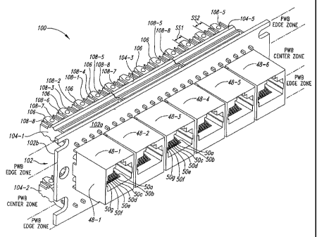
Six jack connectors 48-1 through 48-6 are shown in Figure 3 as being part
of a reduced crosstalk patch panel 100, which is subject of the present
invention. The
patch panel 100 further includes a circuit board 102 having a first side 102a
to fixedly
attach and electrically couple the six jack connectors 48. The circuit board
102 has a
second side 102b to fixedly attach and electrically couple six insulation
displacement
connectors (IDCs) 104-1 through 104-6.
As better shown in Figure 4, each of the IDCs 104 has four separators
106 with each separator having a wire slot 108 on either side of the separator
to receive
two wire ends (not shown) of a conductor wire pair per each of the separators.
When
each of the wire slots 108 receives one of the wire ends, the wire end becomes
electrically coupled to a connector element (not shown) of the IDCS 104 that
is
electrically coupled to the circuit board 102 as further explained below.
Consequently,
each exemplary IDC 104 has eight wire slots 108-1 through 108-8 corresponding
to
pins 1 through 8, respectively, that are electrically coupled through the
circuit board 102
to contact members 50a - 50h, respectively, of one of the jack connectors 48
corresponding to pins 1 through 8, respectively.
As discussed, implementations reduce near end cross talk (NEXT)
through added capacitance so that slot spacing ssl between wire slots 108-1
108-2,
108-3 108-6, 108-5 108-4, and 108-7 108-8 and slot spacing ss2 between 108-2
108-3,
108-4 108-1, 108-6 108-7, and 108-8 108-5 can be the same as conventional IDC
contact spacing such as for category 5 implementations in which the spacing is
0.150
inches with a tolerance of plus/minus 0.005 inches or a smaller tolerance such
as of
plus/minus 0.003 inches while still satisfying the NEXT requirements of the
Category 6
specification involving the NEXT limit line described above.
In the exemplary embodiment of Figure 3, the jack connectors 48 of the
patch panel 100 conform to the industry standard specifications for an RJ45
jack as
controlled by the Federal Communications Commission under Title 47, Part 68.
Performance of exemplary implementations of the patch panel 100 is also to
conform to
Telephone Industries Association Category 5 and 6 enhanced standards. However,
the
principles discussed are applicable to other patch panels using other
communication
connectors.
CA 02547029 2006-05-19
WO 2005/053324 PCT/US2004/039377
I he industry standard external configuration allows the jack connectors
48 of the patch panel 100 to readily connect with an industry standard version
of the
plug connector 40, such as shown in Figure 2E. While described as a jack
connector, it
is noted that the jack connectors 48 of the present invention may take the
form of a plug
or a receptacle, or any other style connector to physically mate with a
corresponding
communication connector prone to produce crosstalk. The patch panel 100 is
configured to provide compensation for both forward and reverse crosstalk
originating
in the conventional plug connectors 40 as near-end crosstalk or in circuits on
the IDC
side of the patch panel as far-end crosstalk.
The 'conventional development of Category 6 component compliant patch
panels per TIA-568-B.2-1 for near-end crosstalk involves understanding the
nature of
the crosstalk created in RJ45 plugs and applying cancellation techniques in
the patch
panels. The cancellation techniques include introducing crosstalk of opposite
polarity to
that created in the plug connector through capacitance and inductance added
and/or
modified in the patch panel.
Factors that add and/or modify capacitance and inductance in the patch
panel include arrangement of tines of jack connectors, sizing of jack
connectors,
placement of signal traces found within the circuit board 102 and the IDCs
104, and
adding interdigitated capacitors found within the circuit board.
As discussed, twisted pair signaling uses pairs of wires with a first wire of
the pair designated as "tip" and the second wire of the pair designated as
"ring." The
voltage and currents found on each "tip" wire and each "ring" wire of a pair
are of
opposite polarity where the "tip" wire of a "tip"-"ring" pair of wires is at a
positive voltage
relative to the "ring" wire of the pair. These opposite polarity aspects of
twisted pair
?5 signaling are used by the described implementations to reduce crosstalk. In
particular,
to compensate for crosstalk caused by a first capacitive coupling between two
wires, a
second capacitive coupling between the two wires can be purposefully added at
a
second location to produce crosstalk having a magnitude opposite to the
crosstalk
found at the first location. Since the first coupling and the second coupling
result in
crosstalk with opposite polarity, the crosstalk associated with the first
coupling and the
crosstalk associated with the second coupling tend to cancel each other
resulting in
substantially reduced levels of crosstalk.
Thus, to compensate for a first crosstalk originating in the plug connector
40, a second crosstalk could be introduced at the patch panel 100 of an equal
amount
11
CA 02547029 2006-05-19
WO 2005/053324 PCT/US2004/039377
and with an opposite polarity with respect to the first crosstalk. Some
conventional jack
designs use capacitive coupling of a polarity opposite to the polarity of
unwanted
coupling found in the conventional plug connector 40 to deliberately introduce
crosstalk
having polarity opposite to the polarity of the unwanted crosstalk originating
in the
conventional plug connector.
According to the terminology used herein, capacitive coupling between
two wires of the same polarity, such as between two "tip" wires or between two
"ring"
wires, is referred to as positive capacitive coupling, whereas capacitive
coupling
between two wires of opposite polarity, such as between a "tip" wire and a
"ring" wire, is
referred to as negative capacitive coupling. Capacitance produced with
parallel plates
and capacitance produced by closely spaced lengths of wire are conventional
methods
used to achieve capacitive coupling opposite in polarity of and to compensate
for
unwanted capacitive coupling. Conventional approaches have taken an approach
in
mitigating crosstalk that crosstalk between various conductor pairs of the
plug
connectors could be considered as having nearly identical magnitudes and thus
symmetrically arranged.
Implementations of the patch panel 100 capacitively compensate the IDC
104. In order to explain how this is done a review of the physical pin order
of the
conventional plug connector 40 and the conventional physical pin order of the
wire slots
108 of the IDC 104 would be helpful. As shown in Figure 2D, the physical pin
order for
the conventional plug connector 40 is pin 1 tip (IT), pin 2 ring (2R), pin 3
tip (3T), pin 4
ring (4R), pin 5 tip (5T), pin 6 ring (6R), pin 7 tip (7T), and pin 8 ring
(8R). The
conventional physical pin order for the wire slots 108 of the IDC 104 is 5T,
4R, IT, 2R,
3T, 6R, 7T, and 8R (not shown). Given the physical pin order of the IDC 104,
pin pairs
adjacent other pin pairs are most influenced by the capacitive properties of
the IDC,
that is, pin 4 - pin 5 pair adjacent pin 1 - pin 2 pair (45-12 pair
combination), pin 1 - 2
pair adjacent pin 3 - pin 6 pair (12-36 pair combination), and pin 3 - pin 6
pair adjacent
pin 7 - pin 8 pair (36-78 pair combination).
Given the conventional physical pin order of the conventional plug
connector 40 and the conventional physical pin order of the wire slots 108 of
the IDC
104 as described above, the following is provided to describe how capacitances
in the
IDC 104 resulting from these adjacent pin pair combinations are addressed. For
the
45-12 pair combination, pin 4R and pin IT are nearest each other and dominate
the
capacitive coupling due to their proximity in the IDC 104. The polarity of the
crosstalk is
12
CA 02547029 2006-05-19
WO 2005/053324 PCT/US2004/039377
the opposite of that created in the conventional plug connector 40 for this
pair
combination. Unfortunately, the IDC pair combination is electrically too far
away to
effectively cancel the plug crosstalk. As a result, this IDC crosstalk is
locally canceled
in the IDC 104 and cancellation of the plug crosstalk applied nearer to the
plug/tine
interface. To address this IDC crosstalk, one interdigitated capacitor, EZ15,
as shown
in Figure 5, is added to electrically couple between pin 5T and pin IT of the
IDC 104
and one interdigitated capacitor, EZ24, is added to electrically couple
between pin 4R
and pin 2R.
For the 12-36 pair combination, pin 2R and pin 3T are nearest each other
and dominate the capacitor coupling due to their proximity in the IDC 104. The
polarity
of this crosstalk is the same as that created in the conventional plug
connector 40 for
the 12-36 pair combination. As a result, much of this crosstalk must be
canceled.
Some same-polarity capacitance at this location is used in combination with a
capacitor
of opposite polarity at the interface (not shown) of the slots 108 and the
circuit board
102 to provide a more effective cancellation of the plug crosstalk. Use of the
IDC
capacitance in this way helps to minimize the size of crosstalk canceling
capacitors.
The capacitive crosstalk created within this IDC pair combination is partially
canceled
by applying interdigitated capacitance. Two capacitors are used: one, EZ13,
between
pin 1T and pin 3T and one, EZ26, between pin 2R and pin 6R. The size of these
capacitors is small as possible to reduce the return loss penalty incurred due
to the
lower than normal impedance of the IDC 104.
For the 36-78 pair combination, pin 6R and pin 7T are nearest each other
and dominate the capacitive coupling due to their proximity in the IDC 104.
The polarity
of this crosstalk is the same as that created in the conventional plug
connector 40 for
this pair combination. As result, much of this crosstalk must be canceled
similarly as
done with the 12-36 pair combination discussed above. Two capacitors are used,
one,
EZ37, between pin 3T and pin 7T and one, EZ68, between pin 6R and pin 8R. The
size of these capacitors is kept as small as possible to reduce the return
loss penalty
incurred due to the lower than normal impedance of the IDC 104. As shown in
Figure
5, other interdigitated capacitors are added to the circuit board 102 to
address crosstalk
produced in areas other than the IDC 104.
Additionally, signal routing at the interface of the circuit board 102 and the
IDC 104 can include aspects to improve the return loss performance of the IDC.
In
some implementations, the IDC 104 has inherently low impedance due to the
close
13
CA 02547029 2006-05-19
WO 2005/053324 PCT/US2004/039377
proximity and relatively large area of its contacts. To counter this low
impedance, a
high impedance section of each of the pairs: pin 4 - pin 5, pin 1 - pin 2, pin
3 - pin 6,
and pin 7 - pin 8, is included near this interface of the circuit board 102
and the IDC
104. Each high impedance section is made by increasing the space between the
traces of each of the pairs, which also helps to improve NEXT performance.
How values for the added capacitances are determined for a given
configuration of the patch panel 100 can be based upon an iterative process
where
capacitance is added to the circuit board, measurements are made, and then
further
addition or subtraction of capacitance is done depending upon analysis and so
on. An
iterative approach can be useful to determine proper capacitances to be added
to the
circuit board 102 since values for the inherent capacitances in the plug
connector 40
and the IDC 104 may be affected by capacitances found elsewhere. With some
exemplary implementations, refinements to determine proper values to use for
the
capacitances to be added to the circuit board 102 can be accomplished through
an
iterative process utilizing both electromagnetic simulation modeling software
with finite
element analysis known in the art and furnished by Ansoft Corporation,
Pittsburgh, PA
running on an HP J5000 Unix computer and with electronic test analyzer
equipment
furnished by Hewlett Packard Corporation including models HP 4380S96, HP
4396B,
and HP 4380A. For some tests, the test analyzer was connected to wire pairs 1 -
4
connected to the plug connector 40. The plug connector 40 was coupled to the
patch
panel 100 through the physical engagement mechanism of the jack connector 48.
With the mentioned exemplary implementation, the electromagnetic
simulation modeling software can be generally used to test ideas for
particular layout
designs for the circuit board 102. The electronic test analyzer can be used
further to
test design layouts and to further refine layout dimensions to achieve
reductions in
crosstalk. The test analyzer can be used to send signals to the patch panel
100
through the conventional plug connector 40 on a first pair of wires connected
to the
conventional plug connector and then can be used to measure resultant amounts
of
crosstalk occurring on second, third, and fourth pairs of wires connected to
the patch
panel. Both near-end crosstalk and far-end crosstalk can be measured and
refinements to the circuit board 102 can be made until reductions in both near-
end
crosstalk and far-end crosstalk to satisfy category 6 performance were
achieved with
the patch panel 100 coupled to the conventional plug connector 40.
An exemplary implementation of the circuit board 102 is shown in Figure 6
14
CA 02547029 2006-05-19
WO 2005/053324 PCT/US2004/039377
as having first and fourth wire trace layers 120 and 136 made from 2.0 oz
finished
copper, second and third wire trace layers 126 and 130 made from 2.0 oz
finished
copper, a first dielectric layer 128 being 0.028 inches thick and having a
dielectric
constant of 4.0, and first and second bonding material layers 124 and 132
being 0.009
inches thick. As shown in Figure 6, an order of layering for the circuit board
102 is as
follows: the first wire trace layer 120, the first bonding material layer 124,
the second
wire trace layer 126, the first dielectric layer 128, the third wire trace
layer 130, the
second bonding material layer 132, and the fourth wire trace layer 136.
The wire trace of the first wire trace layer 120 of the depicted
implementation is shown in Figure 7. The first wire trace layer 120 includes a
first
plurality of wire connector pads (referred to herein as "the plurality of jack
pads").
Selected pads of the plurality of jack pads are labeled in Figure 7 with the
pin number
and jack connector number of the contact member 50 of the jack connector 48 to
which
the pad is electrically coupled. For example, one of the plurality of jack
pads shown on
Figure 7 and labeled pin 1 of 48-4 would be electrically coupled to the
contact member
50a associated with pin 1 of the jack connector 48-4 of the patch panel 100.
The first wire trace layer 120 also includes a second plurality of wire
connector pads (referred to herein as "the plurality of IDC pads"). Selected
pads of the
plurality of IDC pads are labeled in Figure 7 with the pin number associated
with one of
the wire slots 108 and its connector element (such as pin 1 is associated with
wire slot
108-1 and its connector element) of the IDC 104. For example, one of the
plurality of
IDC pads shown in Figure 7 and labeled pin 1 of 104-4 would be electrically
coupled to
the connector element associated with the wire slot 108-1 of the IDC 104-4 of
the patch
panel 100. The plurality of jack pads and the plurality of IDC pads are
similarly labeled
on the second, third, and fourth wire trace layers 126, 130, and 136 shown in
Figures 8,
9, and 10, respectively, and extend through holes formed in the circuit board
102.
One purpose for the first wire trace layer 120 is to add capacitive coupling
using interdigitated wire traces as is done with capacitive wire trace
portions shown in
Figure 7 providing the CZ14, CZ46, CZ47, EZ15, EZ24, EZ26, EZ34, EZ37, and
EZ68
board capacitances shown as part of the circuit diagram of Figure 5.
The second wire trace layer 126 is shown in Figure 8 and the third wire
trace layer 130 is shown in Figure 9 as having wire trace connections between
the
plurality of jack pads and the plurality of IDC pads, each connection
corresponding to a
particular pin number of a particular jack and its corresponding IDC. For
instance, as
CA 02547029 2012-04-10
shown in Figure 8, a connection exists between pin 2 of 48-1 and pin 2 of 104-
1.
In Figure 10, exemplary implementations of compensation are shown only
for jack connectors 48-2, 48-4, and 48-6 and not for jack connectors 48-1, 48-
3, and 48-
5. The fourth wire trace layer 136 adds capacitive coupling with capacitive
wire trace
portions shown in Figure 10 providing the EZ13, CZ23, CZ25, CZ35, EZ56, and
CZ58
capacitances for the jack connectors 48-2, 48-4, and 48-6, but not for the
jack
connectors 48-1, 48-3, and 48-5. For the exemplary circuit board 102 of
Figures 6-10,
none of the center zone or edge zone capacitances depicted in Figure 5 have
been
implemented for the jack connectors 48-1, 48-3, and 48-5. Further
implementations of
the patch panel 100 also use interdigitated wire traces to add capacitance
whereas
other embodiments use other ways of adding capacitance known in the art such
as
through discrete capacitive components.
It should also be noted that the patch panel 100 can be made in a wall
mount version and other versions including those that are free-standing. The
principles
of the present invention are intended to encompass all such variations of
communication connectors. In addition, the present invention is intended to
encompass
communication connectors other than the RJ45 style, and may be designed to
include a
greater or lesser number of twisted pair cables.
From the foregoing it will be appreciated that, although specific
embodiments of the invention have been described herein for purposes of
illustration,
various modifications may be made without deviating from the scope of the
invention.
Accordingly, the invention is not limited except as by the appended claims.
16