Note : Les descriptions sont présentées dans la langue officielle dans laquelle elles ont été soumises.
CA 02548936 2006-06-08
WO 2005/063621 PCT/N02004/000003
1
Title of Invention
Silicon Feedstock for Solar Cells
Technical field
The present invention relates to silicon feedstock for wafers for solar
cells, wafers for solar cells, solar cells and a method for the production of
silicon feedstock for the production of wafers for solar cells.
Background technology
In recent years, photovoltaic solar cells have been produced from ultra
pure virgin electronic grade polysilicon (EG-Si) supplemented by suitable
scraps, cuttings and rejects from the electronic chip industry. As a result
of the recent downturn experienced by the electronics industry, idle
polysilicon production capacity has been adapted to make available
lower cost grades suitable for manufacturing PV solar cells. This has
brought a temporary relief to an otherwise strained market for solar
grade silicon feedstock (SoG-Si) qualities. With demand for electronic
devices returning to normal levels, a major share of the polysilicon
production capacity is expected to be allocated back to supply the
electronics industry, leaving the PV industry short of supply. The lack of
a dedicated, low cost source of SoG-Si and the resulting supply gap
developing is today considered one of the most serious barriers to further
growth of the PV industry.
In recent years, several attempts have been made to develop new
sources for SoG-Si that are independent of the electronics industry value
chain. Efforts encompass the introduction of new technology to the
current polysilicon process routes to significantly reduce cost as well as
the development of metallurgical refining processes purifying abundantly
available metallurgical grade silicon (MG-Si) to the necessary degree of
purity. None have so far succeeded in significantly reducing cost of
production while providing a silicon feedstock purity expected to be
required to match the performance of PV solar cells produced from
conventional silicon feedstock qualities today.
When producing PV solar cells, a charge of SoG-Si feedstock is
prepared, melted and directionally solidified into a square ingot in a
specialised casting furnace. Before melting, the charge containing SoG-
Si feedstock is doped with either boron or phosphorus to produce p-type
CA 02548936 2006-06-08
WO 2005/063621 PCT/N02004/000003
2
or n-type ingots respectively. With few exceptions, commercial solar
cells produced today are based on p-type silicon ingot material. The
addition of the single dopant (eg. boron or phosphorus) is controlled to
obtain a preferred electrical resistivity in the material, for example in the
range between 0.5-1.5 ohm cm. This corresponds to an addition of 0.02
- 0.2 ppma of boron when a p-type ingot is desired and an intrinsic
quality (practically pure silicon with negligible content of dopants) SoG-Si
feedstock is used. The doping procedure assumes that the content of the
other dopant (in this example case phosphorus) is negligible (P< 1/10 B).
If a single doped SoG-Si feedstock of a given resistivity is used in various
addition levels the charge, the addition of dopant is adjusted to take into
account the amount of dopant already contained in the pre-doped
feedstock material.
Singel doped feedstock qualities of n- and p-type can also be mixed in
the charge to obtain a so-called "compensated" ingot. The type and
resistivity of each component of the charge mix must be known to obtain
desired ingot properties.
After casting, the solidified ingot is cut into blocks with the footprint of
the
resulting solar cells for example with a surface area of 125 mm X 125
mm). The blocks are sliced into wafers deploying commercial multi-wire
saw equipment.
PV solar cells are produced from the wafers in a number of process
steps of which the most important are surface etching, POC13 emitter
diffusion, PECVD SiN deposition, edge isolation and the formation of
front and back contacts.
Description of invention
By the present invention it has now been found that PV solar cells
meeting commercial efficiency targets can be produced from a SoG-Si
feedstock produced from metallurgical grade silicon by means of
metallurgical refining processes specifically designed for the PV solar
feedstock application.
CA 02548936 2009-02-26
3
Thus according to a first aspect, the present invention relates to a silicon
feedstock for producing directionally solidified Czochralski, float zone or
multicrystalline silicon ingots, this sheets and ribbons for the production of
silicon wafers for PV solar cells, comprising a silicon feedstock containing:
between 0.3 and 5.0 ppma boron, between 0.1 and 10 ppma phosphorous,
less than 150 ppma of metallic elements, and less than 100 ppma carbon
distributed in the material.
According to a preferred embodiment the silicon feedstock contains
between 0.5 and 3.5 ppma phosphorous.
According to another preferred embodiment, the silicon feedstock (SoG-Si)
comprises less than 50 ppma metallic elements.
The silicon feedstock of the present invention differs substantially from a
charge mix composed of various boron or phosphorous containing silicon
feedstock qualities as described above in that it contains higher levels of
both boron and phosphorous. It has surprisingly been found that the silicon
feedstock of the present invention can be used to produce solar cells
having an efficiency as good as commercial solar cells produced from
electronic grade silicon.
The silicon feedstock of the present invention can be used to produce
directionally solidified Czochralski, float zone or multicrystalline silicon
ingots or thin silicon sheet or ribbon for making wafers for solar cells
having
high efficiency. Silicon ingots, this sheets or ribbons produced from the
silicon feedstock will contain between 0.2 ppma and 10 ppma boron and
between 0.1 ppma and 10 ppma phosphorous, and will have a
characteristic type change from p-type to n-type or from n-type to p-type at
a position between 40 and 99% of the ingot height or sheet or ribbon
thickness. The resistivity profile of directionally solidified ingots produced
form the feedstock of the present invention is described by a
CA 02548936 2006-06-08
WO 2005/063621 PCT/N02004/000003
4
curve having a starting value between 0.4 and 10 ohm cm where the
resistivity value increases towards the type change point.
According to a second aspect, the present invention relates to a
directionally solidified Czochralski, float zone or multicrystalline silicon
ingot or thin silicon sheet or ribbon for making wafers for solar cells,
wherein the silicon ingot, thin sheet or ribbon contains between 0.2 ppma
and 10 ppma boron and between 0.1 ppma and 10 ppma phosphorus
said silicon ingot having a type change from p- type to n-type or from n-
type to p-type at a position between 40 and 99 % of the ingot height or
sheet or ribbon thickness and having a resistivity profile described by a
curve having a starting value between 0.4 and 10 ohm cm and where the
resistivity value increases towards the type change point.
According to a preferred embodiment the silicon ingot, thin sheet or
ribbon has a resistivity starting value of between 0.7 and 3 ohm cm.
According to a third aspect, the present invention relates to a method for
the production of silicon feedstock for producing directionally solidified
Czrochralski, float zone or multicrystalline silicon ingots, thin silicon
sheets or ribbons for the production of silicon wafers for PV solar cells
which method is characterized in that metallurgical grade silicon
produced in an electric arc furnace by carbothermic reduction furnace
and containing up to 300 ppma boron and up to100 ppma phosphorus is
subjected to the following refining steps:
a) treatment of the metallurgical grade silicon with a calcium-silicate
slag to reduce the boron content of the silicon to between 0.2
ppma and 10 ppma;
b) solidifying the slag treated silicon from step a);
c) leaching the silicon from step b) in at least one leaching step by
an acid leach solution to remove impurities;
d) melting the silicon from step c);
e) solidifying the molten silicon from step d) in the form of an ingot by
directional solidification;
f) removing the upper part of the solidified ingot from step e) to
provide a silicon ingot containing 0.2 to 10 ppma boron and 0.1 to
10 ppma phosphorus;
g) crushing and/or sizing the silicon from step f).
CA 02548936 2006-06-08
WO 2005/063621 PCT/N02004/000003
It has been found that the silicon feedstock produced according to this
method is well suited for the production of directionally solidified ingots,
thin sheets and ribbons for the production of wafers for solar cells having
5 an efficiency comparable to commercial solar cells.
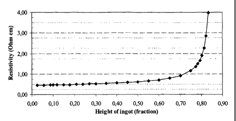
Short description of the drawings
Figure 1 is a diagram showing the resistivity as a function of ingot height
for a first silicon ingot according to the invention, and,
Figure 2 is a diagram showing the resistivty as a function of ingot height
for a second silicon ingot according to the invention.
Detailed description of invention
Example I
Production of silicon feedstock
Commercial metallurgical grade silicon produced by carbothermic
reduction in electric arc furnace was treated with a calcium silicate slag
to remove mainly boron. Boron was extracted from the molten silicon to
the slag phase. The silicon was solidified with very pure silicon crystals
while impurities stayed in the melt until most of the silicon was solidified.
Impurities ended up on the grain boundaries in the solidified silicon.
The solidified silicon was subjected to acid leaching whereby the
intergranular phases was attacked and dissolved together with the
impurities. The remaining undissolved granular silicon was melted and
further refined to adjust the composition before crusting an sieving to
obtain the silicon feedstock for solar grade silicon.
By the method above, two charges of silicon feedstock were produced.
The boron and phosphorus content of the two samples of silicon
feedstock are shown in Table 1.
CA 02548936 2006-06-08
WO 2005/063621 PCT/N02004/000003
6
Table 1
Sample No. ppma boron ppma phosphorus.
1 3.3 3.2
2 1.2 1.1
Example 2
Production of directionally solidified silicon ingot, wafers and solar cells
Silicon feedstock produced according to the method described in
Example 1 was used to produce two directionally solidified silicon ingots
according to the invention. Commercial multicrystalline Si-wafers were
used as reference. A Crystalox DS250 furnace was used for producing
the ingot. A circular quartz crucible with an inner diameter of 25.5 cm
and 20 cm height capable of containing about 12 kg of feedstock was
used. The grown ingots were squared to 100 cm2 and 156 cmZ blocks,
and then sliced into wafers by a saw. From these blocks, a large number
of wafers with thickness in the range of 300-330 m were produced for
cell processing.
The content of boron and phosphorus at 20% height of the two ingots
are shown in Table 2.
Table 2 Chemical analysis for ingot # 1 and 2 at 20% of the height.
Ingot No. ppma boron ppma phosphorus.
1 2.8 1.3
2 1.0 0.3
The bulk resistivity of the as cut wafers was measured through all blocks
by four-point probe on at least each fifth wafer from bottom to top. The
bulk resistivity profile of ingot No 1 and 2 is shown in Figure 1, and
Figure 2 respectively. Figure 1 and 2 show that the resistivity is
substantially constant from the bottom of the ingot and up to about 3/ of
the height of the ingot when the material changes from p-type to n-type.
CA 02548936 2006-06-08
WO 2005/063621 PCT/N02004/000003
7
The type of majority carriers in the silicon block was determined by
qualitative Seebeck coefficient measurement. Hall-and resistivity
measurements using van der Paw geometry were applied to obtain
resistivity, carrier concentration and mobility on selected wafers from top,
middle and bottom of each ingot.
All wafers were etched by NaOH for 9 minutes at 800 for saw damage
removal, followed by flushing in deionized water, HCI, deionized water
and 2% HF.
In order to study the effect of light trapping, isotexturisation was applied
instead of NaOH etching on selected as-cut wafers. This method
combines the removal of the surface saw damage on the as cut wafer
and applies a surface texturisation in one step.
Solar cells were fabricated by POCI3 emitter diffusion, PECVD SiN
deposition, and edge isolation by plasma etching. The front and back
contacts are made by screen printing and then firing through.
The efficiency of the fabricated solar cells are shown in Table 3.
Efficiencies up to r1=14,8% (ingot #2) were reached, which exceed the
efficiency values of the reference material. Commercial monocrystalline
Si wafers were used as reference for comparison.
Table 3:
Ingot Area Efficency best cell
# [cm2] [%]
1 156 14.3
2 156 14.8
Com Ref 156 14.6
The result from Table 3 shows that solar cells having a efficiency
comparable to and even higher than commercial solar cells can be
obtained by the silicon feedstock and the directionally silidified silicon
ingots according to the present invention.