Note : Les descriptions sont présentées dans la langue officielle dans laquelle elles ont été soumises.
CA 02557641 2006-08-28
WO 2005/084218 PCT/US2005/006008
SYSTEM AND METHOD FOR DATA MANIPULATION
FIELD OF INVENTION
[0001] The present application is based on and derives priority from U.S.
Provisional Application No. 60/548,110, filed February 27, 2004, the entire
contents of
which are incorporated herein by reference.
[0002] The present invention relates to systems and methods for data
manipulation
as well as systems that incorporate a data manipulation device.
BRIEF DESCRIPTION OF THE DRAWINGS
[0003] The inventions claimed herein are exemplified in several embodiments.
These exemplary embodiments are described in detail with reference to the
drawings.
These embodiments are non-limiting exemplary embodiments illustrated in
several views
of the drawings, in which like reference numerals represent similar parts
throughout, and
wherein:
[0004] Fig. 1 depicts a high level functional block diagram of a data
manipulation
device, according to an embodiment of the present invention;
[0005] Fig. 2 depicts a high level functional block diagram of a memory
controller
for controlling data storage and access in a memory, according to an
embodiment of the
present invention;
[0006] Fig. 3 depicts a high level functional block diagram of a processor
deployed
in a data manipulation device, according to an embodiment of the present
invention;
[0007] Fig. 4 depicts a functional block diagram of a backup storage in a data
manipulation device, according to an embodiment of the present invention;
CA 02557641 2006-08-28
WO 2005/084218 PCT/US2005/006008
[0008] Fig. 5 depicts a functional block diagram of a battery system in a data
manipulation device, according to an embodiment of the present invention;
[0009] Fig. 6 depicts an exemplary organization of a memory, according to an
embodiment of the present invention;
[0010] Fig. 7 depicts a high level functional block diagram of a data access
request
handler in relation to various flags and LTJN structures, according to an
embodiment of the
present invention;
[0011] Fig. ~ shows exemplary system states and transitions thereof under
different operational conditions, according to an embodiment of the present
invention;
[0012] Fig. 9 depicts an exemplary arrangement of different components of a
data
manipulation device, according to an embodiment of the present invention;
[0013] Fig. 10 illustrates an exemplary arrangement of memory boards and
internal organization thereof, according to an embodiment of the present
invention;
[0014] Fig. 11 shows exemplary arrangement of registered buffers on memory
boards, according to an embodiment of the present invention;
[0015] Fig. 12 shows exemplary arrangement of phase locked loop clocks on
memory boards, according to an embodiment of the present invention;
[0016] Fig. 13 depicts exemplary pin shift arrangement between two different
memory boards, according to an embodiment of the present invention;
[0017] Fig. 14(a) shows an exemplary physical layout of a SCSI controller
board
SCB, according to an embodiment of the present invention;
[0018] Fig. 14(b) shows an exemplary physical layout of a DRAM controller
board or DCB, according to an embodiment of the present invention;
[0019] Fig. 14(c) shows an exemplary physical layout of memory chips on a
memory board, according to an embodiment of the present invention;
CA 02557641 2006-08-28
WO 2005/084218 PCT/US2005/006008
[0020] Fig. 14(d) shows an exemplary physical arrangement of different boards
of
a data manipulation device in a compact box, according to an embodiment of the
present
invention;
[0021] Figs. 14(e) and (f) show different exploded perspective views of an
exemplary physical assembly of different boards and components of a data
manipulation
device, according to an embodiment of the present invention;
[0022] Fig. 14(g) and (h) show different perspective views of an exemplary box
hosting a data manipulation device with different connection ports, according
to an
embodiment of the present invention;
[0023] Fig. 15(a) and (b) illustrate different exemplary embodiments of
storage
systems where one or more data manipulation devices are used as high speed
disk storage
emulators, according to an embodiment of the present invention;
[0024] Fig. 16 is a flowchart of an exemplary process, in which a data
manipulation device is used to emulate a high speed disk for data storage and
access,
according to an embodiment of the present invention;
[0025] Fig. 17 is a flowchart of an exemplary process, in which a data
manipulation device is initialized, according to an embodiment of the present
invention;
[0026] Fig. 18 is a flowchart of an exemplary process, in which a processor in
a
data manipulation device receives a data access request and forwards the
request to
appropriate drivels), according to an embodiment of the present invention;
[0027] Fig. 19 is a flowchart of an exemplary process, in which a data request
is
handled out of a memory, according to an embodiment of the present invention;
[0028] Fig. 20 is a flowchart of an exemplary process, in which a data request
is
handled from either a memory or a backup storage, according to an embodiment
of the
present invention;
CA 02557641 2006-08-28
WO 2005/084218 PCT/US2005/006008
[0029] Fig. 21 is a flowchart of an exemplary process, in which a diagnosis is
performed and error messages are recorded in a backup storage, according to an
embodiment of the present invention;
[0030] Fig. 22 shows an. exemplary deployment configuration in which one or
more data manipulation devices are deployed as slave processing units to
perform high
speed data off loading tasks, according to an embodiment of the present
invention;
[0031] Fig. 23 shows an exemplary deployment configuration in which a data
manipulation device is deployed to assist network switches to perform high
speed traffic
control and network management processing, according'to an embodiment of the
present
invention; and
[0032] Fig. 24 shows an exemplary deployment configuration in which data
manipulation devices are deployed to handle high bandwidth data transmission
over high
speed network connections, according to an embodiment of the present
invention.
DETAILED DESCRIPTION OF SEVERAL EMBODIMENTS
[0033] The processing described below may be performed by a properly
programmed general-purpose computer alone or in connection with a special
purpose
computer. Such processing may be performed by a single platform or by a
distributed
processing platform. In addition, such processing and functionality can be
implemented in
the form of special purpose hardware or in the form of software or firmware
being run by
a general-purpose or network processor. Thus, the operation blocks illustrated
in the
drawings and described below may be special purpose circuits or may be
sections of
software to be executed on a processor. Data handled in such processing or
created as a
result of such processing can be stored in any memory as is conventional in
the art. By
way of example, such data may be stored in a temporary memory, such as in the
RAM of a
CA 02557641 2006-08-28
WO 2005/084218 PCT/US2005/006008
given computer system or subsystem. In addition, or in the alternative, such
data may be
stored in longer-term storage devices, for example, magnetic disks, rewritable
optical
disks, and so on. For purposes of the disclosure herein, a computer-readable
media may
comprise any form of data storage mechanism, including such existing memory
technologies as well as hardware or circuit representations of such structures
and of such
data.
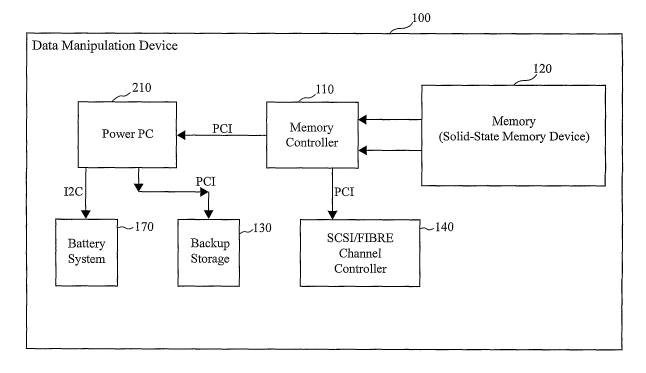
[0034] Fig. 1 depicts a high level functional block diagram of a data
manipulation
device (DMD) 100, according to an embodiment of the present invention. The DMD
100
comprises a channel controller 140, which can be either a SCSI channel
controller, Fibre
channel controller, on other interface controller available within the art, a
memory
controller 110 that controls data storage and access of a memory 120, a backup
storage
system 130, low power CPU such as a Power PC (210) and a battery system 150.
The
SCSI/Fibre/interface channel controller 140 in the DMD 100 is responsible for
interfacing
with the outside world. The nature of the interactions between the DMD 100 and
the
outside world may depend on the purpose the DMD 100 is deployed and the
functional
role of the DMD 100 in the context of the deployment. For example, the
SCSI/Fibre (or
other interface within the art) channel controller 140 may interface with one
or more host
systems when the DMD 100 is deployed to emulate high speed solid state disk
storage. In
this case, the DMD 100 receives a data request through the SCSI/Fibre channel
controller
140 from a host system and then accesses data at a high speed based on what is
requested.
When the DMD 100 is deployed as a slave data manipulation device to perform
designated applications, it may interface, also via its SCSIlFibre/interface
channel
controller 140, with a master server that, for example, may invoke the DMD 100
to
perform a massive query search in data stored on the DMD 100.
CA 02557641 2006-08-28
WO 2005/084218 PCT/US2005/006008
[0035] In the DMD 100, the channel controller 140 may provide a common driver
to access either SCSI or Fibre channel or other interface to data buses. That
is, each
implementation of the DMD 100 may deploy either any common interface
controller using
the same driver. Deployment of any controller may be determined based on where
and
how the deployed DMD product is to be used.
[0036] The common driver may support a SCSI interface that may comply with
Ultra320 and have backward compatibility with Fat SCSI, Ultra SCSI, Ultra2
SCSI, and
Ultra160 SCSI. A 16-bit parallel SCSI bus may perform 160 mega transfers per
second
that may yield a 320 Mbytes/second synchronous data transfer rate. The common
driver
may also support a dual 2-Gbit Fibre Channel (FC) interfaces and provide
backward
a,
compatibility with 1-Gbit FC. The DMD 100 may also provide a RS-232 interface
(not
shown in Fig. 1) for a commercial line interface (CLI).
[0037] A data request received by the channel controller is directed to the
memory
controller 110, which then processes the data request. A data request may
include a read
request or a write request, which may involve, for example, either writing a
new piece of
data or updating an existing piece of data. Depending on the system state at
the time the
data request is received, the memory controller 110 may accordingly carry out
the data
request from appropriate storage(s). For instance, the memory controller 110
may perform
the requested data access directly from the memory 120, from the backup
storage 130, or
from both.
[0038] When the data request is completed, the DMD 100 sends a response,
through the channel controller 140, back to the underlying requesting host
system. A
response may include a piece of data read from the DMD 100 based on the
request or a
write acknowledgment, indicating that data that was requested to be written to
the DMD
CA 02557641 2006-08-28
WO 2005/084218 PCT/US2005/006008
100 has been written as requested. The response to a read request may also
include a
similar acknowledgement indicating a successful read operation.
[0039] The DMD 100 may be deployed for different purposes. For example, it
may be used to emulate a standard low profile 3.5" high-density disk (HDD). In
this case,
it may identify itself to the outside world, through a SCSI/Fibre bus, as such
a standard
device so that the interacting party from the outside world may invoke
appropriate
standard and widely available devices or drivers to interact with the DMD 100.
The DMD
100 may then employ solid state memory 120 to allow the unit to be utilized as
a solid
state disk (SSD).
[0040] The memory controller 110 controls the operations performed in the
memory 120. Under normal circumstances, data requests from host systems are
carried
out with respect to the memory 120. In certain situations such as when the
memory load is
not yet completed, data access operations may need to be performed from
somewhere
other than the memory 120. For instance, when the DMD 100 is in a restore
system state,
a read request may be performed temporarily from the backup storage 130. In
this case,
through the Power PC (210), the memory controller 110 may also control data
operations
performed in the backup storage 130. Details related to the memory controller
110 are
discussed with reference to Figs. 2 and 3.
[0041] The backup storage 130 in conjunction with battery 170, provides a self
contained and non-volatile backup storage to the DMD 100. Such a storage
process may
be used to backup data stored in the memory 120 when, for example, power to
the DMD
100 is low or down. The backup storage 130 may also be used to store or record
diagnostic information obtained during a diagnosis procedure so that such
recorded
diagnostic information may be retrieved or accessed off line when it is needed
to, for
instance, determine system problems. Such a storage space may also be used as
a
CA 02557641 2006-08-28
WO 2005/084218 PCT/US2005/006008
transitional memory space when memory load is not yet completed. Details
related to this
aspect are discussed with reference to Figs. 4 and 8.
[0042] The battery system 170 in the DMD 100 provides off line power to the
DMD 100. The battery system may be crucial in facilitating data back up from
the
memory into the backup storage 130 when the power is persistently low or down.
Details
related to the battery system are discussed with reference to Fig. 5.
[0043] The memory 120 may comprise a plurality of memory banks organized on
one or more memory boards. Each memory bank may provide a fixed memory
capacity
and dynamic random access (DRAM). Different memory banks may be addressed in a
coherent manner. The memory 120 may also be organized into a plurality of
logic unit
number (LUN) structures and each of such structures may support variable block
sizes.
Memory allocation may be performed by the memory controller 110 according to
various
criteria. Details related to memory organization are discussed with reference
to Figs. 6
and 7.
[0044] Fig. 2 depicts a high-level functional block diagram of the memory
controller 110, according to an embodiment of the present invention. The
memory
controller 110 comprises a processor 210, a PCIX Bus Interface (I/F) 250, a
DRAM
controller 260 with Error Correcting Circuitry (ECC) circuitry 270, and a DRAM
connector 280. The processor 210 may be realized using a commercially
available
general-purpose, low power central processing unit (CPS. For example, the 400
MHz
32-bit PowerPC 405GPr micro-controller from IBM Core. may be used as the
processor
210, which has a real time cloclc 240 capable of 600 MIPS at 400 MHz clock
rate. The
32-bit 405GPr micro-controller (processor 210) has a single device on the
processor local
bus that provides a certain amount (e.g., 32 MB) of SDRAM (220) with a bus
width of 32
CA 02557641 2006-08-28
WO 2005/084218 PCT/US2005/006008
bits. The processor 210 may also have its own boot flash device (230) on the
local bus
that provides a certain amount (e.g., 32 MB) of non-volatile flash memory with
a flash
data bus width of 16 bits. The real-time clock may be provided for different
purposes such
as time stamping error logs, long interval timing for battery charge, power
loss filtering,
etc.
[0045] The PCIX Bus I/F 250 may be used to adapt the PCIX bus transfer rate
and
burst length to the transfer rate and burst length required for the memory 120
(e.g., double
data rate synchronous dynamic random access (DDR SDRAM)). The DRAM controller
260 may perform various functions related to memory access. For example, it
may
provide, through the ECC circuitry 270, single bit error correction and double
bit error
detection and support 8-bit ECC over the 64 bit data from the memory 120. The
DRAM
controller 260 may also generate interrupts to the processor 210 whenever it
detects a
memory error. Furthermore, it may also provide refresh cycles and refresh
cycle timing.
In one embodiment, the DRAM controller may also carry out power saving
strategies,
controlled by the processor 210, by sending signals to memory banks to control
the
memory modes. This will be discussed in detail with reference to Fig. 3. The
DRAM
connector 280 provides a physical connection between the memory controller 110
and the
memory 120.
[0046] Fig. 3 depicts a high-level functional block diagram of the processor
210,
according to an embodiment of the present invention. The processor 210 employs
an
operating system 300 installed and running thereon, an initializer 365, a PCIX
bus
interface 330, a data access request handler 335, a memory status controller
340, a restore
mechanism 345, a memory backup handler 350, a read request handler 355, and a
write
request handler 360. The processor 210 may also include a diagnostic mechanism
305,
which is responsible for performing various diagnostic routines, and an error
logging
CA 02557641 2006-08-28
WO 2005/084218 PCT/US2005/006008
mechanism 310, which is responsible for writing error messages to the backup
storage
130.
[0047] The operating system 300 rnay be a commercially available product such
as
Linux. Upon a start-up (or reset) of the system, the operating system 300 may
be Loaded
from the backup storage 130. Upon being booted, the operating system 300 may
invoke
the initializes 365 to perform various initializations. The initializes 36S
may be 'responsible
for initializing the memory arrays, the backup storage drive, and the
SCSI/Fibre/other
interface system. Boot images for these devices may be downloaded to the
respective
device during the initialization. To ensure that the initialized devices are
functioning
properly, the initializes 365 may also invoke the diagnostic mechanism 305 to
perform
certain diagnostic routines.
[0048] The diagnostic mechanism 305 may perform diagnostic routines according
to some pre-determined diagnostic configuration (320). Such configuration may
be
dynamically revised to satisfy application needs. When components are added or
removed
from the DMD 100, the diagnostic configuration may need to be changed
accordingly.
For example, if more memory boards are added, the configuration for,diagnosis
may
reflect the additional device.
[0049j When the diagnostic mechanism 305 performs diagnosis routines, it rnay
send a signal to a device, configured to be tested, and then compare a
response from the
tested component with some anticipated result 325. If the measured result
differs from the
anticipated result, an error message may be generated and the error logging
mechanism
310 may be invoked to record the diagnostic information in the backup storage
130. In
some embodiments, the diagnostic mechanism 305 may also be invoked through
manual
activation (302) via the shell of the operating system 300.
to
CA 02557641 2006-08-28
WO 2005/084218 PCT/US2005/006008
[0050] If the diagnosis is completed successfully, the initializer 365 may
then
register to receive signals from various drivers and invoke the restore
mechanism 345 to
perform restore operations, including copy data from the backup storage 130 to
the
memory 120. When the restore operation is completed, the initializer 365 may
then
change the system state to an appropriate state for data access operations.
[0051] The system state of the DMD 100 may be signified through a plurality of
flags 315. For example, when the initializer 365 changes the system state to
restore, it
may set a "restore" flag 315-1 indicating the system is restoring data or a
memory load is
being performed. When the restore mechanism 345 completes the memory load, it
may
reset the same flag 315-1, indicating that the memory load is completed.
Similarly, if the
system is performing a backup operation (e.g., moving data from the memory 120
to the
backup storage 130), a "backup" flag may be set. Different system states may
indicate
where data is currently stored. Therefore, depending on the system state, a
data request
may be handled differently.
[0052] The PCIX bus interface 330 is used to communicate with the controller
140, the backup storage 130, and the memory arrays 120. When the controller
140
forwards a data request from a host system to the memory controller 110, the
data request
is channeled through the PCIX connection between the controller 140 and the
PCIX bus
interface 330 of the processor 210.
[0053] Upon receiving the data request, the PCIX bus interface 330 sends the
data
request to the data access request handler 335. The data access request
handler 335 may
analyze the request and then activate the read request handler 355, if the
request is a read
request, or the write request handler 360, if the request is a write request.
Depending on
the system state, the read and write request handlers 355 and 360 may operate
differently.
For example, if a data read request is received before a restore operation
(memory load) is
11
CA 02557641 2006-08-28
WO 2005/084218 PCT/US2005/006008
completed, the read request handler 355 may direct a read instruction to the
backup
storage 130 instead of sending such an instruction to the memory 120. If a
data write
request is received before memory load is completed, the write request hander
360 may
send a write instruction to both the memory 120 and the backup storage 130 and
then
receive an acknowledgement only from the backup storage 130.
[0054] The memory backup handler 350 is responsible for carrying out memory
backup operations. This handler may be activated in certain scenarios such as
when a
persistent power loss is detected or when battery power drops to a certain
level. When it is
activated, it may set the "backup" flag, indicating a system state transition
to a backup
system state. Under this system state, the DMD 100 may refuse a data request
received
from a host system. This system state may not change until, for example, a
steady power
return is detected.
[0055] The memory status controller 340 is responsible for carrying out a
power
saving scheme of the memory banks. In one embodiment of the present invention,
to
reduce power consumption and hence heat generation, the DMD 100 employs a
power
saving scheme in which different memory banks are put into different modes,
some of
which yield lower power consumption. The implementation of the power saving
scheme
may depend on the system state. In some embodiments, when the system is in a
"normal"
or "restore" mode, the processor 210 may put, through the memory status
controller 340,
all memory banks, except one active bank, into a "sleep" or "power down" mode.
With
DDR SDRAM memory, the wake up time can be about 3 microseconds (compared with
30 microsecond for SDR SDRAM). Such a significantly shorter wake up time
facilitates
higher speed storage accesses. While in the "sleep" mode, an inactive memory
bank may
still receive clocking. The power saving scheme is also applied to special DDR
memory
120 chips which have been developed to increase storage capacity density in
the space of a
12
CA 02557641 2006-08-28
WO 2005/084218 PCT/US2005/006008
standard size DDR chip form factor. This special DDR memory chip is developed
by the
stacking of multiple memory die in such a manner as to allow each die to be
address as a
single chip though it is physically located inside a single form factor.
[0056] When the system is in "backup" mode, the processor 210 may further
reduce power consumption by stopping the sending of clocking to the inactive
memory
banks and putting the inactive memory banks in a "self refreshing" mode of
operation.
Although it may take longer (about 20 microseconds) to exit the "self
refreshing" mode,
such a longer wake-up time may be acceptable in a backup situation.
[0057] Fig. 4 depicts a functional block diagram of the baclcup storage 130,
according to an embodiment of the present invention. The backup storage 130
includes a
backup storage disk 420 and a backup disk controller 410. The controller 410
is
connected to the PCIX bus and is responsible for controlling data storage and
access
to/from the disk 420. The disk may be implemented as a rotating disk or a high-
density
disk (HDD). The capacity of the disk may be determined based on application
needs. The
backup storage 130 may be used not only for backup purposes but also for other
purposes
such as being used as memory when a memory load is not yet completed,
recording
diagnostic information or error messages, or mirroring data written to DDR 120
memory.
[0058] In conventional systems, a typical restoration period may range from 1
to 2
minutes per gigabyte. During the restoration period, systems typically cannot
respond to
any data request. This causes a delay. In some embodiments of the present
invention,
since the backup storage 130 is used as the memory before a memory load is
completed, it
eliminates the delay. In addition, in one embodiment, the DMD 100 is running
under a
Linux operating system with its own SDR.AM and this further improves the speed
of this
operation. For instance, for 12 Gigabytes of memory, it can take about 5
minutes to
13
CA 02557641 2006-08-28
WO 2005/084218 PCT/US2005/006008
complete the operation. Details related to using the backup storage 130 as
memory prior
to completion of memory load are discussed with reference to Figs. 8, 15, and
19
'[0059] The backup storage 130 may also be used to log error messages in the
event
of failure and diagnostic information obtained when diagnostic routines are
carned out. In
the event of system failure, the error information logged in the backup
storage 130 may be
removed for assessing the cause of the failure.
[0060] Fig. 5 depicts a functional block diagram of the battery system 150,
according to an embodiment of the present invention. The battery system 150
comprises a
battery 500 with a built-in gas gauge 540, a DC-DC converter 510, a monitor
530, and a
battery charger 520. The monitor 530 is responsible for monitoring the
condition of the
battery 500 through the gas gauge 540. The monitoring results may be used to
determine
whether the system state needs to be changed. For example, when the battery
power is
persistently going down and reaches a certain low threshold, the system state
may be
changed from a "normal" state to a "backup" state.
[0061] The battery 500 may output certain, voltages such as 7.2v. The battery
charger 520 is responsible for recharging the battery when it is needed. The
DC-DC
converter 510 is responsible for converting the battery output voltage, e.g.,
7.2v or SCSI
power of 12v, into different voltages needed in the system. For example, the
DC-DC
converter 510 may take input voltage of 7.2v or 12v and convert into 1.2v,
1.25v, 1.8v,
2.Sv, 3.0v, or 3.3v.
[0062] In some embodiments of the present invention, the battery system 150
may
be controlled by the general purpose processor 210 in the memory controller
110. A
monitoring scheme may be carried out under the control of the general purpose
processor
210 for the purpose of prolonging the life of the battery. Under this scheme,
the monitor
530 monitors the power level of the battery 500. The observed power level is
sent to the
14
CA 02557641 2006-08-28
WO 2005/084218 PCT/US2005/006008
general purpose processor 210. When the power level reaches certain level
(e.g., full
power), the general purpose processor 210 may stop the charging until the
power falls to a
certain lower level (e.g., 90%). This prevents the battery to be charged
continuously when
it is already at a full power level (which is known to shorten the life of the
battery). In
addition, when the monitored power level reaches a low threshold, the general
purpose
processor 210 may cause the device to automatically shut down.
[0063] Fig. 6 depicts an exemplary organization of the memory 120, according
to
an embodiment of the present invention. The memory 120 may comprise one or
more
memory boards. Each of the memory boards may include a plurality of memory
banks.
For example, one memory board may include memory banks 610-1, 610-2, 610-3,
620-1,
620-2 and 620-3. Another memory board may include memory banks 630-1, 630-2,
630-3, 640-1, 640-2 and 640-3.
[0064] Each memory board may also include a plurality of registers and clocks
such as phase locked loop (PLL) clocks. Thus, the one memory board includes
chip
select/clock select devices 610 and 620 to provide clocking to memory banks
610-1,
610-2, 610-3 and 620-1, 620-2 and 620-3, respectively. The other memory board
includes
chip select/clock select devices 630 and 640 to provide clocking to memory
banks 630-l,
630-2, 630-3 and 640-1, 640-2 and 640-3.
[0065] The memory 120 may also be logically organized into a plurality of LUN
structures. The DMD 100 may support multiple LUN structures capable of
handling
varying block sizes. Different LUN structures may facilitate different block
sizes. In
addition, each LUN structure may also support different block sizes. With such
capabilities, the DMD 100 may appear to have multiple storage devices, each
with a
certain block size. This enables the DMD 100 to interface with host systems
that require
different block sizes.
is
CA 02557641 2006-08-28
WO 2005/084218 PCT/US2005/006008
[0066] When variable block sizes are supported, a data request from a host
system
with a required block size may be first mapped to a LUN structure that has a
matching
block size. Fig. 7 depicts a high-level functional block diagram of the data
access request
handler 335 in relation to various flags 315 and multiple LUN structures 700,
according to
an embodiment of the present invention. As discussed earlier, a data request
may be
processed in different internal storage media (e.g., out of the memory 120,
out of the
backup, storage, or both) and a determination may be made based on the system
state. In
addition, depending on where the data request is being handled, appropriate
LUN
structures may be accordingly identified.
[0067] In the exemplary embodiment illustrated in Fig. 7, the memory is
organized
into, for example, M LUN structures, LUN 1 700-1, LUN 2 700-2, ..., and LUN M
700-
M. The data access request handler 335 comprises a system flags retriever 710,
an LUN
initializer 720, a system state determiner 730, an LUN mapping mechanism 740,
an
operating device determiner 750, and various data access operators, including,
for
instance, a memory read operator 760-1, a memory write operator 760-2, a
backup storage
read operator 770-1, and a backup storage write operator 770-2.
[0068] The LUN initializer 720 may be responsible for initializing the
multiple
LUN structures 700. For example, when the system is initially set up, all the
LUN
structures may be set with a uniform or a standard block size (e.g., 512
bytes) and this
initial block size may later be changed to satisfy data requests with
different block size
values. For instance, some systems I~(e.g., Unisys products) may operate on a
block size of
180 bytes and some (e.g., Tandem products) may operate on a block size of 514
bytes.
[0069] Upon receiving a data request, the data access request handler 335 may
first
access, via the system flags retriever 710, the flags 315, which indicate the
operational
status of the system. The system flags retriever 710 may then forward the
retrieved flag
16
CA 02557641 2006-08-28
WO 2005/084218 PCT/US2005/006008
values to the system state determiner 730 to identify a current system state.
Based on the
determined system state, the operating device determiner 750 may decide the
devices)
(e.g., the memory 120 or the backup storage 130 or both) from/to where the
read/write
operation is to be performed. For example, when the system flags indicate a
normal
system state, the operating device determiner 750 may select the memory 120 as
the
operating device, i.e., a data request, either a read request or a write
request, will be
handled out of the memory 120.
[0070] When the system flag "restore" is raised indicating that memory load is
not
yet completed, the operating system determiner 750 may select to handle a read
and a
write request differently. For example, a read request may be carried out from
the backup
storage 130 because the data to be read may still be in the backup storage
130. As for a
write request, the system may write the same data to both the memory 120 and
the backup
storage 130 in order to ensure data integrity. The system state determined by
the system
state determiner 730 may also be used by the LUN mapping mechanism 740 to map
the
data request to a particular LUN structure.
[0071] Based on the decision in terms of from/to where the read/write
operation is
to be carried out, the operating device determiner 750 may invoke an
appropriate data
I
request operator. For example, when a data readlwrite request is to be
processed out of the
memory 120, the memory read/write operator 760-1/760-2 may be activated. When
a data
read/write request is to be processed out of the backup storage 130, the
backup read/write
operator 770-1/770-2 may be activated.
[0072] In addition, based on the LUN mapping result, the LUN mapping
mechanism 740 may also supply relevant information to the invoked operator.
For
example, the LIJN mapping mechanism 740 may forward the information related to
the
mapped LLTN structure to the activated operator.
1~
CA 02557641 2006-08-28
WO 2005/084218 PCT/US2005/006008
[0073] An activated operator may send some data operation instructions to an
appropriate device and then receive a response from the device after the data
operation is
completed. Such a response may include the return of a piece of data (e.g.,
when data is
read), an acknowledgement (e.g., a write acknowledgement), or an error message
(e.g.,
from either a read operation or a write operation). The response is from a
respective
device to which the operation instructions are sent: For example, to read a
piece of data to
satisfy a corresponding read request, a read operator (either the memory read
operator
760-1 or the backup read operator 770-1) may send a read instruction with an
appropriate
address (e.g., within a specific LUN structure determined by the LUN mapping
mechanism 740) to the underlying operating device. When the read is completed,
the read
operator may receive the data read from the operating device with or without
some
acknowledgement message. The received data and the acknowledgement, if any,
may
then be sent to the PCIX bus interface 330 (see Fig. 3) to be forwarded to the
requesting
host system. When an error has occurred during the operation, the read
operator may also
receive and forward the error message.
[0074] When a write operation is involved, depending on whether the operation
is
handled out of the memory 120 only (e.g., in a normal system state) or out of
both the
memory 120 and the backup storage 130 (e.g., in a restore system state), the
write operator
may behave differently. In a normal system state, the memory write operator
760-2 is
invoked for a write operation. The memory write operator 760-2 may first send
a write
instruction with data to be written and then wait to receive either an
acknowledgement or
an error message from the memory 120. Upon receiving a response, the memory
write
operator 760-2 forwards the received information to the PCIX bus interface
330.
[0075] In some other system states (which will be discussed with reference to
Fig.
8 below), a write operation is performed in both the memory 120 and the backup
storage
18
CA 02557641 2006-08-28
WO 2005/084218 PCT/US2005/006008
130. In this case, both the memory write operator 760-2 and the backup write
operator
770-2 are invoked. Both write operators send the data to be written with write
instructions
(e.g., where to write) to their respective operating devices (i.e., the memory
120 and the
backup storage 130). Since the memory 120 may operate at a much higher speed
than the
backup storage 130, only the backup write operator 770-2 may be configured to
forward
the write acknowledgement or error message received from the backup storage
130 to the
PCIX bus interface 330, even though the memory write operator 760-2 may also
receive
such information from the memory 120.
[0076] Fig. 8 shows various exemplary system states and transitions thereof
under
different operational conditions in the DMD 100, according to an embodiment of
the
present invention. The state transition table 800 contains rows and columns.
Rows
correspond to current system states 810 and columns correspond to events or
conditions
820 under which a current state transits to a different state or remains in
the same system
state. Each entry in the table 800 corresponding to a particular row and a
particular
column represents the next system state, given the current system state
represented by the
row and the event/condition represented by the underlying column.
[0077] In the table 800, there are 9 exemplary system states, including a boot
state
810-1, labeled as (1), a restore state 810-2, labeled as (2), a in-service-
backup state 810-3,
labeled as (3), a in-service state 810-4, labeled as (4), a in-service-baclcup-
pending state
810-5, labeled as (5), a restore-backup-pending state 810-6, labeled as (6), a
backup state
810-7, labeled as (7), an idle state 810-8, labeled as (8), and an off state
810-9, labeled as
(9). There are various events/conditions which may trigger system state
transitions,
including the event of memory array failure 820-1, backup failure 820-2, no
power 820-3,
power on 820-4, battery drop/backup 820-5, battery riselbackup 820-6, power
loss 820-7,
persistent power loss 820-8, and persistent power return 820-9.
19
CA 02557641 2006-08-28
WO 2005/084218 PCT/US2005/006008
[0078] Each system state indicates a particular system operational condition.
For
example, the boot state (1) indicates that the DMD 100 is going through a
booting process
triggered by, for example, power on, reset, or via some software means. The
restore state
(2) indicates that the DMD 100 is restoring data from the backup storage to
the memory or
is simply loading the memory. The in-service-backup state (3) indicates that
the memory
120 is not functioning properly (due to, for instance, memory failure, or
insufficient
battery for backup) and a data request will be serviced from the backup
storage. The in-
service state (4) indicates that the DMD 100 is operating under a normal
situation. That is,
all data requests are handled out of the memory 120.
[0079] The in-service-backup-pending state (5) may indicate a situation in
which a
data request is serviced but with a pending backup. That is, although data
requests are still
handled out of the memory 120, there exists some condition (e.g., power drop)
that is
being monitored and that may trigger a backup procedure in the near future.
The restore-
backup-pending state (6) may indicate that the system is performing a memory
load
(restoring data from the backup storage to the memory) and some existing
condition/event
(e.g:, power loss) may trigger a backup procedure in the near future if the
condition
persistently gets worse (e.g., persistent power loss). The backup state (7)
simply indicates
that the DMD 100 is performing a bacleup procedure by moving data from the
memory
120 to the backup storage 130. The idle state (8) indicates that the system is
currently idle
and not accepting any data request. The off state (9) indicates that the DMD
100 is
currently off.
[0080] Each system state may cause the DMD 100 behave differently in terms of
how to handle a data request. For example, in system states in-service (4) and
in-service-
backup-pending (5), a data request is always serviced from the memory 120. In
system
states restore (2), in-service-backup (3), and restore-backup-pending (6), a
data request
CA 02557641 2006-08-28
WO 2005/084218 PCT/US2005/006008
may be serviced from either the memory 120 or from the backup storage 130 or
both,
depending on the nature of the request and the location of the data requested.
In system
states boot (1), backup (7), idle (8), and off (9), no data request is
serviced.
[0081] System states change under certain conditions/triggering events. Given
a
fixed current state, the DMD 100 may transit to different system states when
different
events occur. Fox example, at the boot state (1), if memory failure occurs
(820-1), the
system state transits from boot state (1) to the in-service-backup state (3).
That is, all data
requests will be handled out of the backup storage 130 due to the memory array
failure. If
a backup storage 130 failure occurs (820-2) during booting, the system state
may transit
from a boot state (1) to an idle state (8) because the boot process cannot go
fizrther without
the backup storage 130. If the current system state is normal (in-service
state (4)) and a
power loss is detected (820-7), the system state may transit to the in-service-
backup-
pending state (5). In this state, although the system is still in service,
there is a possible
pending backup. In this state, if the power loss persists (820-8), the system
state further
transits to the backup state (7). There are certain cells in the'table 800
that have blank
entries indicating that, given the current state, the underlying event
represented by the
column does not apply. For example, when the system is in an off state,
certain events
such as memory array failure 820-1 and backup storage failure 820-2 will not
affect the
system state.
[0082] Fig. 9 depicts an exemplary organizational arrangement 900 of different
components of the DMD 100, according to one embodiment of the present
invention. The
exemplary organizational arrangement 900 includes five separate physical
parts, including
a SCSI/Fibre controller board (SCB) 910, a DRAM controller board (DCB) 940, a
memory board (MB) 950, a high-density disk 930 providing the backup storage
space, and
a battery 920.
21
CA 02557641 2006-08-28
WO 2005/084218 PCT/US2005/006008
(0083] Some components of the same logical organization discussed earlier may
be grouped on different boards. For example, the backup storage disk
controller 410 may
be realized using an at-attachment (ATA) controller (7), which may be arranged
physically
separate from the backup storage disk 930 (e.g., implemented using a Toshiba
1.8" 20 GB
high density disk (labeled as 9) in the exemplary arrangement shown in Fig. 9.
Similarly,
the DC-DC converter 510 (see Fig. 5), the battery charger 520, and the monitor
530 may
be arranged on the SCB 910, separate from the battery 500 and the gas gauge
540. The
exemplary arrangement may be made based on factors other than the logical or
functional
organization considerations such as size, heat consumption, and whether a
component
needs to be arranged at a location so that it can be easily replaced.
Alternatively, or in
addition, the physical organizational arrangement may be designed based on
considerations related to the compactness of the entire system.
[0084] The SCSIlFibre controller board (SCB) 910 includes an ATA controller
chip 7, the SCSI/Fibre controller chip 6, and a power manager and converter
chip 3 that
contains a DC-DC converter, a battery charger, and a monitor. The DRAM
controller
(DCB) 940 includes a general processor chip (e.g., a 32 bit 405 GPr) 12, a
SDRAM chip
16, a boot flash memory 17, a real-time clock 18, and a field programmable
gate arrays
(FPGA) chip 11 programmed as both the PCIX bus I/F 11-1 and the DRAM
controller
with ECC circuitry 11-2 (discussed with reference to Fig. 2).
[0085] Each board may also contain different parts that facilitate connections
among different boards and components. For example, the SCB 910 includes an
ATA
connector 8 facilitating the connection between the ATA controller chip 7 and
the backup
disk 9, a PCIX connector 10 facilitating the PCIX connection between the SCB
910 and
the DCB 940, a SCSI/Fibre connector 2 providing physical connections between
the
SCSI/Fibre controller and the SCSI/Fibre backplane (1), and a battery
connector 4
22
CA 02557641 2006-08-28
WO 2005/084218 PCT/US2005/006008
connecting the SCB 910 to the battery 5. Similarly, the DCB 940 includes a
counterpart
PCIX connector 10 facilitating the connection to the PCIX connector on the SCB
910, a
DRAM connector 19 facilitating the connection between the DRAM controller 11-2
and
the memory board 950, an RS232 connector providing a serial connection point
between
the outside and the DMD 100, LED lights 14 providing a means to show system
status and
activity, and a reset button 15 facilitating the need for resetting the system
from outside.
[0086] According to one embodiment, the FPGA 11 is connected directly with the
PCIX connector 10. This enables the DMD 100 to perform data transfers through
its on-
board FPGA to accomplish high speed storage access without going through the
general
processor 12. In addition, since the PCIX comlector 10 is also connected to
the SCSI
controller 6, the FPGA 11 can transfer data directly from/to outside sources
without going
through the general processor 12. This makes the storage not only accessible
at a high
speed but also shared as well. Furthermore, since the general processor 12 can
be
implemented using a commercially available CPU deployed with commercial
operating
system (e.g., Linux), the DMD 100 is a full-fledged computer, which is capable
of
supporting various applications normally run on conventional general-purpose
computers.
In this case, applications may run on the general processor 12 and data
necessary for the
applications may be transferred to the SDRAM of the processor 12.
[0087] Figs. 10-13 illustrate an exemplary arrangement of memory boards and
their internal organization, according to an embodiment of the present
invention. In one
embodiment, the memory 120 may comprise one or more memory boards, each of
which
may include three or six memory banks. Different memory banks within a memory
board
and different memory boards may be connected in certain fashion to facilitate
uniform
addressing and clocking. Fig. 10 shows how two exemplary memory boards, a
memory
board 0 1010 and a memory board 1 1020, are connected with the DRAM controller
on the
23
CA 02557641 2006-08-28
WO 2005/084218 PCT/US2005/006008
DCB 940. The memory board 0 1010 comprises six memory banks, a bank 0 1010-1,
a
bank 1 1010-2, a bank 2 1010-3, a bank 3 1010-4, a bank 41010-5, and a bank 5
1010-6.
The six banks are linked together and connected to the DCB 940 through a
memory board
connector 1005-1. Similarly, the memory board 1 1020 includes six memory
banks, a
bank 0 1020-l, a bank 1 1020-2, a bank 2 1020-3, a bank 3 1020-4, a bank 4
1020-5 and a
bank 5 1020-6. The six banks on the memory board 1 1020 may be similarly
connected
together and to the memory board 0 1010 via a memory connector 1005-2. The
memory
board 1 1020 is connected to the DCB 940 through the memory board 0 1010.
[0088] The memory board connectors 1005-1 and 1005-2 may enable different
types of signal passing. For example, it may allow data to pass through. It
may also
enable address information to pass through. In addition, it may allow control
signals to
pass through. In some embodiments, memory board connectors contain a 72-bit
data bus
with 64 bits data and 8 bits ECC, data strobes, and data mask signals. They
may be routed
in a similar fashion. The memory board connectors may also include an address
bus and
additional paths for control signals. Address and control signals may
terminate on each
board by a register buffer, which may be clocked by a clock specifically for
the board.
[0089] Fig. 11 shows an exemplary arrangement of register buffers in memory
boards, according to an embodiment of the present invention. In Fig. 11, each
memory
board has one register buffer. The memory board 0 1010 has a register buffer
1110 and
the memory board 1 1020 has a register buffer 1120. Each may be clocked
differently to
intercept address and control signals designated to the underlying memory
board. Each
memory board may use a different clock (CK), clock enable (CKE) signal, and
chip select
(CS) signal. Each memory bank may have separate CKE and CS signals. Each
memory
board may have one or more clocks, each of which may be implemented as a phase
locked
loop (PLL) clock.
24
CA 02557641 2006-08-28
WO 2005/084218 PCT/US2005/006008
[0090] Fig. 12 shows an exemplary arrangement of PLL clocks in memory boards,
according to an embodiment of the present invention. In the illustration, a
memory board
1200 has two PLL clocks, 1210 and 1220, each of which is responsible for, for
example,
three memory banks. In the illustrated embodiment, PLL clock 1210 is
responsible for
clocking bank 3 1200-4, bank 4 1200-5 and bank 5 1200-6, and PLL clock 1220 is
responsible for clocking bank 0 1200-1, bank 1 1200-2 and bank 2 1200-3.
[0091] To accommodate routing signals through a DCB-MB-MB traverse, a
memory board may be designed to facilitate pin shift. One exemplary pin shift
scheme
between two memory boards is illustrated in Fig. 13, according to an
embodiment of the
present invention. To route signals between two memory boards with six memory
banks
(A, B, C, D, E and F), each of the memory boards may have 28 pins on each
side. Among
the 28 pins used to connect the memory board 0 1010 to the DCB 940, 14 pins
are for
signal routing between the DCB 940 and the memory board 0 1010 and the other
14 pins
are for signal routing between the DCB 940 and the memory board 1 1020.
[0092] Among the first set of 14 pins dedicated for connecting to the memory
board 0 1010, 6 pins are for CKE signals for each of the six memory banks
(CKEOA,
CKEOB, CKEOC, CKEOD, CKEOE and CKEOF), 6 pins are for CS signals for each of
the
six memory banks (CSOA CSOB, CSOC, CSOD, CSOE and CSOF), and 2 pins are for
clocking the two PLL cloclcs where CLKOAB for clocking a PLL 1310 responsible
for
banks A, B and C, and CLKOCD for clocking a PLL 1320 responsible for banks D,
E and
F. These pins are located at (starting from the right most as the first
position) positions
7-12 (for CKEOA - CKEOF), 15-16 (for CLKOAB and CLKOCD), and 17-22 (for CSOA -
CSOF).
[0093] The remaining 14 pins are for connecting the DCB 940 and the memory
board 1 1020. Six pins at positions 1-6 are for the clock enable signals,
CKElA - CKE1F,
CA 02557641 2006-08-28
WO 2005/084218 PCT/US2005/006008
of the six banks on the memory board 1 1020, two pins at positions 13-14 are
for the two
clocking signals, CLK1AB and CLK1CD, for two PLL clocks 1330 and 1340
(responsible
fox clocking banks A, B, C, D, E and F, respectively, of the memory board 1
1020), and
another six pins at positions 23-28 are for chip selections signals, CS1A -
CS1F,
corresponding to the six banks on the second board 1020. Signals dedicated to
the second
memory board 1020 are routed through the first memory board 1010 to arrive at
the same
pin positions from where the corresponding signals are routed into the first
memory board
1010. That is, the clock enable signals CKElA - CKE1F are routed into the
memory
board 1 1020 at positions 7-12 (same as the positions for CKEOA - CKEOF), the
clocking
signals CLK1AB and CLK1CD are routed into the memory board 1 1020 at positions
15-16 (same as for CLKOAB and CLKOCD), and the chip selection signals CS1A-
CS1F
are routed into the memory board 1 1020 at positions 17-22 (same as CSOA -
CSOF).
[0094] Fig. 14(a) shows an exemplary physical layout of a SCSI controller
board
SCB 1400, according to an embodiment of the present invention. The SCB 1400
has a
plurality of components including, but not limited to, a SCSI controller clop
such as
53C1030T with 456 pins 1404, an optional heat sink 1401 placed near the SCSI
controller
(e.g., on top of the SCSI controller) to extract the heat away from the SCSI
controller, an
ATA controller 1406 such as chip HP1371N, a backup storage disk 1403 such as
Toshiba
1.8" HDD disk, an ATA connector 1409 (underneath the HDD disk 1403), a DC-DC
power converter 1402 with a battery monitor and a charger, a host SCSI
connector 1408
(or SCSI backplane) through which a host system communicates with the SCSI
controller,
and SCSI connectors 1408-1, 1408-2, 1408-3 that connect the SCSI backplane to
the SCSI
controller. The SCB 1400 may also include an oscillator 1405, and two PCIX
connectors
PKS with 100 pins 1407-1 and 1407-2. Exemplary sizes for various components
and their
operative power level are illustrated in Fig. 14(a).
26
CA 02557641 2006-08-28
WO 2005/084218 PCT/US2005/006008
[0095] Fig. 14(b) shows an exemplary physical layout of a DRAM controller
board or DCB 1410, according to an embodiment of the present invention. The
DCB 1410
physically embodies a general purpose processor chip 1418 such as 405GPr with
456 pins,
an SDR.AM chip 1411, a flash memory chip 1412, a real-time clock chip 1413, an
FPGA
chip 1414 programmed as the PCIX Bus I/F and a DRAM controller, an RS232
interface
1415, two slots for DRAM coimectors, i.e., a PAKS-140 slot 1416-1 and a PAKS-
120 slot
1416-2, and two slots for PCIX connectors to the SCB 1400, i.e., PKS 1417-1
and 1417-2
corresponding to their counterparts 1407-1 and 1407-2 on the SCB 1400.
Similarly,
exemplary sizes and their operative power levels for different components of
the DCB
1410 are also illustrated.
[0096] Fig. 14(c) shows an exemplary physical layout of memory chips on a
memory board 1420, according to an embodiment of the present invention. In the
illustration, there is a total of 36 memory stacks of 3 chips each arranged in
four separate
rows (1421, 1422, 1426, and 1427) with each row having 9 stacks (1421-l, ...,
1421-9,
1422-l, ..., 1422-9, 1426-1, ..., 1426-9, and 1427-l, ..., 1427-9). The four
rows of stacks
1
are aggregated into two groups of 18 stacks residing on each side of the
physical board.
Between the two groups, there are two PLL clocks 1424, a register buffer 1423,
and two
slots for DRAM connectors, i.e., a PAKS-140 1425-1 and a PAKS-120 1425-2
(which
correspond to the counterpart connectors 1416-1 and 1416-2 on the DCB 1410).
The
exemplary physical sizes of each of the components and their operative power
levels are
indicated. Each memory stack may represent a memory capacity of certain number
of
bytes. As discussed earlier, there may be multiple memory boards included in
the DMD
100.
[0097] Fig. 14(d) shows an exemplary physical arrangement of different boards
of
the DMD 100 in a compact box 1430, according to an embodiment of the present
27
CA 02557641 2006-08-28
WO 2005/084218 PCT/US2005/006008
invention. There are a plurality of layers of boards and components arranged
in a compact
manner with considerations related to heat reduction, ease of component
replacement, and
efficiency in connections. According to one embodiment of the present
invention, all
components of he DMD 100 may be packaged in a low profile 3.5" form factor
that is
deployable in any drive bay of any device. The top two layers include two
memory boards
1420-1 and 1420-2, each of which has the memory chip arrangement as described
with
reference to Fig. 14(c). The two memory boards 1420-1 and 1420-2 are connected
via the
corresponding DRAM connectors 1425-1 and 1425-2 or the PADS 140 and PAKS 120
connectors. Below the memory boards resides the DCB 1410, which connects to
the
above memory board (1420-2) via its DRAM connectors 1416-1 and 1416-2 to their
counterparts on the memory board 1420, i.e., 1425-1 and 1425-2 (see Fig.
14(c)).
[0098] Below the DCB 1410 is the SCB 1400 on the bottom of the compact, box
1430. The general-purpose processor chip 405 GPr (1418) is installed on the
bottom side
of the DCB 1410. The internal backup disk 1430 is on the left of the SCB 1400
with an
ATA connector 1409 beneath it. The SCSI controller chip 1404 resides towards
the right
side of the SCB 1400 with a heat sink 1401 on its top. The host SCSI connector
1408 is
located on the bottom right of the compact box 1430. The SCSI connectors 1480-
1, 1408-
2, and 1408-3 connect the host SCSI connector 1408 to the SCSI controller chip
1404.
The SCB 1400 communicates with the DCB 1410 via the PCIX connectors located
and
aligned as counterparts on both boards (1407-1 v. 1417-1, and 1407-2 v. 1417-
2). The two
pairs of PCIX connectors are aligned in front of the SCSI controller chip 1404
and the heat
sink 1401. The ATA controller 1404 is behind these connectors.
[0099] The two memory boards 1420-l and 1420-2 as well as the DCB 1410 are
narrower than the SCB 1400 and installed towards the right side of the compact
box 1430.
28
CA 02557641 2006-08-28
WO 2005/084218 PCT/US2005/006008
On the left of these smaller boards is the battery 1431, which is on the top
left of the SCB
1400.
[00100] Figs. 14(e) and (h) show different views of an implementation of
the DMD 100 box, according to an embodiment of the present invention. In Fig.
14(e),
the DMD box 1440 has various holes distributed to help to dissipate heat. In
this view, the
battery 1431 is on the top right, adjacent to the two memory boards 1420-1 and
1420-2,
and the DCB 1410 and above the backup storage disk 1403 and its ATA connector
1409
(beneath the backup storage disk 1403) on the SCB 1400. The host SCSI
connector 1408
is on the opposite side of the backup storage disk on the SCB 1400.
[00101] In one embodiment of the present invention, the DMD 100 is
packaged in a very compact manner in a box with a low profile 3.5" form
factor. As
indicated earlier, the DMD 100 is a full-fledged computer. Its compact
paclcaging with a
low profile 3.5" form factor makes it deployable in any drive bay of any
device and may
be used in a variety of applications, as discussed in more detail below.
(00102] Fig. 14(f) shows a view that is 90 degree rotated compared with Fig.
14(e). With this view, it can be seen that the SCSI controller chip 1404 is
near the host
SCSI connector 1408 and connected to the host SCSI connector 1408 via SCSI
connectors
1408-1, 1408-2, and 1408-3 (not visible).
[00103] Fig. 14(g) shows a collapsed view of Fig. 14(f). When the boards
are installed and the compact box 1430 is closed, what is seen from the
backplane of the
box is the host SCSI connector 1408, which is located at the same layer as the
SCB 1400
and underneath the DCB 1410 and the two memory boards 1420-1 and 1420-2.
[00104] Fig. 14(h) shows the opposite side of the compact box 1430 when
the boards are installed. The battery 1431 is on the edge of the box, which is
adj acent to
29
CA 02557641 2006-08-28
WO 2005/084218 PCT/US2005/006008
three smaller boards, the memory boards 1420-1 and 1420-2 and above the backup
storage
disk 1403 and its ATA connector 1409 on the SCB 1400.
[00105] The DMD 100 as described above is a data processor in a low
profile 3.5" form factor and it is deployable in any drive bay of any device.
Fig. 1S(a) and
Fig. 15(b) illustrate the DMD 100 deployed as a high speed disk storage
emulator such as
a standard low profile 3.S" high-density disk (HDD). Since the DMD 100 is
capable of
conducting very high speed data movement, using the DMD 100 as a storage
emulator
provides an effective means for massive data storage at a high speed transfer.
Fig. 15(a)
shows an exemplary configuration when the'DMD 100 is deployed as a high speed
dislc
storage emulator for a plurality of host systems, i.e., a host system 1 1 S
10, a host system 2
1520, ..., and a host system K 1530. In this deployment, a host system may
send a data
request to the DMD 100 via its SCSI/Fibre channel controller 140 (see Fig. 1).
Upon
receiving the data request, the DMD 100 processes the data request, accesses
the requested
data, and then sends a reply back to the requesting host system.
[00106] Fig. 1 S(b) shows a different exemplary configuration when the
DMD 100 is deployed as a high speed disk storage emulator. In this
configuration, a
single host system 1 S40 may deploy a plurality of DMDs, i.e., a DMD 1 1560, a
DMD 2
1570, ..., and a DMD K 1580, for massive data storage. To coordinate among the
multiple
DMDs, a dispatcher 1SS0 may be deployed configured to direct data requests
from the
host system 1540 and forward responses from the DMDs to the host system 1540.
Data
stored in the multiple DMDs may be distributed according to various criteria
determined,
for example, according to application needs. For example, different logical
parts of a
database may be stored in different DMDs and a distribution map may be
established and
used by the dispatcher 1550 to determine how to direct requests and forward
responses.
Some of the DMDs may also be provided for fault tolerance purposes.
Alternatively, the
CA 02557641 2006-08-28
WO 2005/084218 PCT/US2005/006008
dispatcher may be configured to perform load balancing before dispatching a
data request
to a particular DMD.
[00107] Fig. 16 is a flowchart of an exemplary process, in which the DMD
100 is used as a high speed disk emulator (e.g., emulating a solid state high
speed disk)
and handles a data request, according to an embodiment of the present
invention. The
system is iutialized first at 1600. At the end of the initialization, an
appropriate system
state is set. Details related to the initialization process are discussed with
reference to Fig.
17. After the initialization, the system receives, at 1605, a data request
from a host
system. Detailed processes relating to receiving a data request are discussed
with
reference to Fig. 18. When the data request is to access (i.e., read or write)
spine data
stored in the DMD 100, the data transfer may be conducted directly through the
FPGA 12
without going through the general processor 12 (as discussed with reference to
Fig. 9). To
service such a data request, the system determines the current system state.
If the system
state is in-service (state (4)) or in-service-backup-pending (system state
(5)), determined at
1610 and 1650, respectively, the data request is handled accordingly, at 1615
from the
memory 120. The process of handling a data request from the memory 120 is
discussed
with reference to Fig. 19.
[00108] If the system state is in-service-backup (system state (3)), restore-
backup-pending (system state (6)), or restore (system state (2)), determined
at 1650, 1665,
and 1670, respectively, the data request is handled accordingly, at 1660, from
either the
memory 120 or the backup storage 130, depending on the location of the data
requested.
Details related to data request processing from either the memory 120 or the
backup
storage 130 are discussed with reference to Fig. 20. If the system state is
one of the
backup states (system state (7)), the idle state (system state (8)), and the
off state (system
31
CA 02557641 2006-08-28
WO 2005/084218 PCT/US2005/006008
state (9)), determined t 1675, 1685, and 1690, respectively, the system
refuses, at 1680, to
serve the data request.
[00109] After the data request is handled (either served at 1615 or at 1660),
the system checks, at 1620, whether a backup needs to be performed. The
conditions under
which a backup process needs to be initiated are discussed with reference to
Fig. 8 (system
state transitions). If a backup is needed, the DMD 100 invokes, at 1625, a
backup process.
During the backup (or restore) process, certain flags may be set at
appropriate times to
enable correct system state transition. For example, when a backup process is
initiated,
the system may set a backup flag so that the system will refuse all subsequent
data
requests prior to the completion of the backup process. Upon completion, the
flag may be
properly reset so that the system state transition may be initiated.
[00110] The system may also check, at 1630, whether certain diagnostic
routines need to be performed. Exemplary criteria related to when to perform
diagnostic
routines are discussed above. For example, a regular interval may be set up so
that such
routines are performed regularly. The diagnostic routines may also be
triggered by some
software applications) upon detection of certain events. Responsible personnel
may also
activate them externally. The diagnostic routines are performed at 1635. If
there is any
error detected during diagnosis, determined at 1640, the error messages are
written or
recorded, at 1645, in the backup storage 130.
[00111] The system may also check, at 1646, whether a restore process
(memory load) needs to be initiated. Exemplary conditions under which a memory
load
process is initiated are discussed with reference to Fig. 8 (system state
transitions). If
restoration is needed, the process is performed at 1647. During this process,
certain flags
may be set to indicate that data is being moved from the backup storage 130 to
the
memory 120 so that a data request received under such a system state can be
handled
32
CA 02557641 2006-08-28
WO 2005/084218 PCT/US2005/006008
properly. Upon completion of the restore process, the flag is reset so that
system state
may be appropriately changed.
[00112] Fig. 17 is a flowchart of an exemplary process, in which the DMD
100 is initialized, according to an embodiment of the present invention. The
operating
system is first booted at 1710. Upon completion of booting the OS, the
processor 210
initializes different drives, including the memory 120, at 1720, the backup
'storage drive, at
1730, and the SCSI/Fibre drive, at 1740. Based on the status of the
initialization, the
system then sets the appropriate system state at 1750.
[00113] Fig. 18 is a flowchart of an exemplary process, in which the
processor 210 receives a data request and forwards the request to appropriate
drivels),
according to an embodiment of the present invention. When the processor,210
receives, at
1810, a data request via its PCIX interface, it first translates, at 1820, the
data request.
Before it forwards the data request to an appropriate drive, the processor 210
determines,
at 1830, the current system state. Based on the current system state and the
nature of the
data request, the processor 210 determines, at 1840, appropriate operating
device from
where the data request is to be handled and subsequently forwards, at 1850,
the data
request to such determined operating device.
[00114] Fig. 19 is a flowchart of an exemplary process, in which a data
request is handled out of the memory 120, according to an embodiment of the
present
invention. Upon receiving a data request, the DMD 100 first maps, at 1900, the
data
request to an appropriate LUN structure based on, for example, the block size
required.
The nature of the data request is then analyzed at 1910. If the data request
is a read
request, a read request is sent, at 1915, to the memory 120. The data is then
read at 1920.
When the data read from the memory 120 is received at 1925, it is returned, at
1930, to the
host system that made the data request. If the data request is a write
request, a write
33
CA 02557641 2006-08-28
WO 2005/084218 PCT/US2005/006008
request with the data to be written is sent, at 1935, to the memory 120. The
data is written,
at 1940, to the memory 120. When the data write is completed, an
acknowledgement is
received, 1945, from the memory 120 and is then forwarded, at 1950, to the
host system
that made the data request.
[00115] Fig. 20 is a flowchart of an exemplary process, in which a data
request is handled from either the memory 120 or the backup storage 130,
according to an
embodiment of the present invention. As discussed earlier, when the system
state is either
in-service-backup (system state (3)), restore-backup-pending (system state
(6)), or restore
(system state (2)), a data request is handled either from the memory 120 or
the backup
storage 130, depending on the location of the data requested. To handle a data
request in
such conditions, the DMD 100 first determines, at 2000, whether the data
request is a read
or a write request.
[00116] If the data request is a read request, the location of the data to be
read is determined at 2005. If the data to be read is located in the backup
storage 130, an
appropriate LUN structure is mapped, at 2010, based on the data request before
a read
request is sent, at 2015, to the backup storage 130. After the data is read,
at 2020, from
the baclcup storage 130, the data is received, at 2025, from the backup
storage 130 and is
then forwarded, at 2030, to the host system that made the read request.
[00117] If the data to be read is located in the memory 120, a read request is
first mapped, at 2035, to an appropriate LIJN structure before the data
request is sent, at
2040, to the memory 120. After the data is read, at 2045, from the memory 120,
it is
received, at 2050, and subsequently forwarded, at 2030, to the requesting host
system.
[00118] If the data request is a write request, determined at 2000, the DMD
100 may perform a write operation in both the memory 120 and the backup
storage 130.
In this case, the write request is first mapped, at 2055, to an appropriate
LUN structure in
34
CA 02557641 2006-08-28
WO 2005/084218 PCT/US2005/006008
both the memory 120 and the backup storage 130. The mapping may be performed ,
according to the block size required. Based on the mapped LUN structure, a
write
instruction and the data to be written are sent, at 2060, to both the memory
120 and the
backup storage 130 and at 2065, the data is then written to both storage
spaces. When a
write acknowledgement is received, at 2070, from the backup storage 130, the
DMD 100
forwards the acknowledgement to the host system that made the write request.
[00119] Fig. 21 is a flowchart of an exemplary process, in which a diagnosis
is performed and error messages are recorded in the backup storage 130,
according to an
embodiment of the present invention. In this exemplary embodiment, the
diagnosis may
be performed one component at a time. To test a component of the DMD 100, a
signal is
first sent, at 2110, from the processor 210 to the component. The processor
210 then
measures, at 2120, the result after the component receives the signal. The
measured result
is then compared, at 2130, with pre-stored anticipated result. If the measured
result does
not match the anticipated result, determined at 2140, it may indicate that the
component is
malfunctioning. In this case, error messages related to the test is written,
at 2150, to the
backup storage 130. The diagnosis process continues until, determined at 2160,
all the
components to be tested have been tested. The diagnosis process then ends at
2170,
[00120] The DMD 100 described herein may also be deployed for other
purposes. For example, DMD may be deployed as a data off load engine or
device. In
such an application, a server may off load its Il0 intensive tasks to a DMD.
Such a DMD
may be required to share data between the DMD and the processor in the server.
Data may
need to be placed at a location that is accessible to both the DMD and the
server. The
DMD so deployed can provide high speed data manipulation according to the
requirement
of the designated tasks because data transfer/movement in DMD may be performed
directly by the FPGA without going through the general purpose processor. Such
an
CA 02557641 2006-08-28
WO 2005/084218 PCT/US2005/006008
application is feasible because the DMD described herein has an open
architecture and
small in size. Therefore it can be easily embedded or connected to the server
without
needing any special device or software connections.
[00121] Fig. 22 illustrates an exemplary configuration in which one or more
slave DMDs are deployed by a master server as data off load engines or
devices. In this
embodiment, a plurality of DMDs (e.g., DMD 1 2230, DMD 2 2240, ..., and DMD k
2250) are deployed by a server 2220 connected to one or more clients (e.g., a
client 2210).
When a client 2210 sends a service request to the server 2220, depending on
the nature of
the request, the server 2220 may direct some of the processing to one of the
DMDs. Since
the DMD described herein is a full fledged computing device, it is capable of
performing
data manipulations and processing at a very high speed. For instance, if a
request is a
query seeking an answer based on a search in a massive database, if the server
is to
perform the search itself, its computation power may be tied up so that the
performance of
the server may degrade. Alternatively, with the illustrated configuration, if
the slave
DMDs store different portions of the database and are configured to run
database
applications, the master server 2220 may direct one of the slave DMDs (which
may have
the appropriate portion of the database data stored therein) to perform the
required massive
search at a high speed. In this way, the master server effectively frees
itself from I/O
intensive tasks and does not have to devote its computation power to perform
the search,
effectively allowing the master server to focus on other services.
[00122] Fig. 23 illustrates another exemplary application of the DMD 100.
In this illustration, a DMD is deployed as a network control mechanism. In
this
configuration, a network node i 2310 is connecting to another network node j
2350 via a
dynamic network path determined by one or more network switches. To do so, a
DMD
2340 may be deployed to provide high speed data manipulation capabilities to
one or more
36
CA 02557641 2006-08-28
WO 2005/084218 PCT/US2005/006008
network switches (e.g., network switch m 2330-1, ..., and network switch n
2330-2). Such
data manipulation tasks include various network control decision making such
as traffic
control and network management such as security and monitoring. In networking,
switches are often required to dynamically direct the traffic based on
information related
to the traffic load and health of the network. Such dynamic network
information is often
analyzed and then flushed out at a rapid speed in order to effectively reflect
the current
state of the network traffic. In addition, information is often required to be
shared among
different switches and to be manipulated at a very high speed. The DMD 100
described
herein is suitable to satisfy those requirements. A DMD deployed in such a
setting may be
equipped with necessary traffic control and/or management features in the form
of, for
instance, software or firmware. The FPGA direct path to access data stored
therein permit
the DMD to carry out data manipulation tasks at a very high speed.
[00123] Fig. 24 illustrates another exemplary application of the DMD 100.
In this embodiment, a DMD may be deployed for high speed data manipulation for
data
transmission and receiving. This may be especially suitable when data
transmission is
related to data of high volume, over a high bandwidth channel such as
multimedia or video
information over a high speed network connections such as optical fiber
network. In this
application, a sender 2410 may be requested by a receiver 2450 to transmit
certain data
stored at the sender site. For example, in Video on Demand (VoD) applications,
a user
may request a service provider to transmit a movie via a cable network. Since
such data is
high in volume and the transmission time is often critical, the sender 2410
may deploy one
or more DMDs (e.g., a DMD 2420) not only for data storage but also for high
speed
transmission. That is, the deployed DMD 2420 may be connected directly to the
high
speed connection 2440 (e.g. the cable network) and is responsible for various
data
operations to be performed prior to data transmission. For example, the
requested data
37
CA 02557641 2006-08-28
WO 2005/084218 PCT/US2005/006008
may need to be encrypted prior to be sent. Since DMD itself is a full fledged
computing
device instead of a passive storage device, a DMD deployed in this setting may
be
equipped with necessary encrypting applications. In addition, due to the FPGA
path for
direct accessing data without going through the general processor and other
features
described (e.g., alternative memory mode scheme), the DMD is capable of
transferring
data in and out of the memory at a very high rate, which is often necessary
for multimedia
and video applications.
[00124] Similarly, at the receiving site, another DMD 2460 may be
deployed to perform high speed receiving and storage. In addition, the DMD
2460 may
also be configured to perform data decryption, which may be performed prior to
saving the
received data in the DMD 2460 or when the stored data is retrieved by the
receiver from
the DMD's storage. For example, a user may request a movie via a Video on
Demand
service and the received movie may be store at the receiver site first in its
encrypted form
and later is retrieved and decrypted for viewing.
[00125] The above discussed examples are merely for illustration. The
DMD 100 described herein has various unique features, including, but is not
limited to,
small in size, compact and open architecture, general data processing
capability because of
its employment of commercial CPU and OS, high speed because of its direct FPGA
access
of memory without going through processor and alternative memory mode scheme,
inclusion of self contained on-board backup storage. These features enable the
DMD 100
to be deployable in a variety of different application scenarios as well as to
be used, each
as a nucleus in a large solid state disk system in a modular fashion. Such a
highly
modularized system is capable of handling multiple file structures within a
single unit,
effective implementation of data integrity, fault isolation, rapid backups and
restoration,
and fault tolerance.
38
CA 02557641 2006-08-28
WO 2005/084218 PCT/US2005/006008
[00126] While the invention has been described with reference to the certain
illustrated embodiments, the words that have been used herein are words of
description,
rather than words of limitation. Changes may be made, within the purview of
the
appended claims, without departing from the scope and spirit of the invention
in its
aspects. Although the invention has been described herein with reference to
particular
structures, acts, and materials, the invention is not to be limited to the
particulars
disclosed, but rather can be embodied in a wide variety of forms, some of
which may be
quite different from those of the disclosed embodiments, and extends to all
equivalent
structures, acts, and, materials, such as are within the scope of the appended
claims.
39