Note : Les descriptions sont présentées dans la langue officielle dans laquelle elles ont été soumises.
CA 02573907 2014-02-04
,
[0001] MEMS DEVICE AND INTERPOSER AND METHOD FOR
INTEGRATING MEMS DEVICE AND INTERPOSER
FIELD OF THE INVENTION
[0002] The invention relates to Microelectromechanical Systems (MEMS) devices
and
methods for integrating the MEMS devices, in particular, to an assembly having
a MEMS
device directly bonded to an interposer and methods for integrating the
assembly.
BACKGROUND OF THE INVENTION
[0003] A Microelectromechanical Systems (MEMS) device, such as a MEMS device
used in a gyroscope or an accelerometer, is typically sensitive to thermal and
mechanical
stresses. In the prior art, the MEMS device is directly mounted to the floor
or substrate of
a ceramic chip carrier package. The MEMS device typically is manufactured from
silicon.
The material from which the package is manufactured typically does not provide
a good
match with the material of the MEMS device in terms of their respective
coefficients of
thermal expansion. Furthermore, the MEMS device typically is bonded to the
package by
brazing. The braze materials may impart similar thermal stress to the MEMS
device.
[0004] One type of prior art device uses an interposer to isolate the MEMS
device from
the package. The interposer is a device upon which a MEMS device is mounted.
The
1
CA 02573907 2007-01-15
WO 2006/019761
PCT/US2005/024763
interposer is in turn mounted in the MEMS package. The function of the
interposer is to
isolate the MEMS device from the mechanical and thermal stress exerted by the
package.
FIG. 1 illustrates a schematic structure of the package, the interposer, and
the MEMS
device. The MEMS device and the interposer are manufactured as two separate
entities.
The MEMS device is subsequently brazed to the interposer using a gold and/or
tin alloy.
One disadvantage of the prior art structure is that the braze materials may
impart thermal
stresses to the MEMS device. Furthermore, the braze materials may creep over
time.
This negatively affects the long term performance stability and reliability of
the MEMS
device.
[0005] Moreover, in the prior art device, the MEMS device typically includes a
substrate
and a silicon device attached to the substrate. The substrate is bonded to the
interposer
by brazing. The substrate is manufactured from glass or other materials. In
the situation
that the substrate is not manufactured from the same material as the silicon
device, the
substrate may also impart thermal stresses to the silicon device. This may
degrade the
performance of the whole system.
[0006] FIG. 2 illustrates a traditional method of producing the MEMS device,
in which
the interposer and the MEMS device are manufacture as two separate entities.
The
process starts from the top of the figure and continues to the bottom of the
figure. The
traditional process of making an interposer starts with a double-side polished
silicon
wafer 10. Oxide layers 12 are grown on both sides of the silicon wafer 10. On
a top side
of the wafer 10, the oxide layer is selectively etched, and ohmic contacts 14
and braze
materials 16 are deposited in the etched area. The MEMS device as denoted by
number
22 generally includes a silicon device 24 attached to a substrate 26.
Typically, the silicon
device 24 is attached to the substrate 26 by anodic bonding. The substrate 26
is then
attached to the interposer 10 by brazing. The traditional materials used in
brazing are
gold and tin. The brazing materials between the substrate 26 and the
interposer 10 may
creep over time, and that may have negative effects on the performance of the
MEMS
device.
2
CA 02573907 2007-01-15
WO 2006/019761
PCT/US2005/024763
[0007] What is needed is a structure having a MEMS device and an interposer,
wherein
the interposer has a thermal expansion well-matched to the MEMS device. There
is a
further need of a method of manufacturing the structure.
SUMMARY ST THE INVENTION
[00051 The present invention provides an assembly comprising a
Microelectromechanical Systems (MEMS) device and an interposer that reduces
the
thermal and mechanical stresses exerted from the interposer or a package of
the assembly
to the MEMS device, and a method for manufacturing the MEMS device and the
interposer assembly.
[0009] According to one aspect of the present invention, the process is based
on a
Bonded and Etch Back Silicon-On-Insulator (referred to hereinbelow as BESOT)
method.
The BESOT method includes providing a Silicon-On-Insulator (SOT) wafer, which
has (i)
a handle layer, (ii) a dielectric layer, which preferably is a silicon dioxide
(Si02) layer,
and (iii) a device layer. The device layer is first patterned by mesa etch.
After the device
layer is patterned, the SOT wafer is bonded to a substrate with the patterned
device layer
facing the substrate. The handle layer and the dielectric layer of the SOI
wafer are
removed by etching. The device layer is further etched to define the MEMS
device. In
the BESOT method, the structure etching is performed after the dielectric Si02
layer is
removed.
[0010] According to another aspect of the present invention, the method
comprises
manufacturing an interposer and manufacturing a MEMS device together with
bonding
the MEMS device with the interposer. The process of manufacturing the
interposer starts
from obtaining an SOT wafer. A thin oxide layer is formed on a bottom surface
of the
handle layer of the SOT wafer. The oxide layer is etched to define holes or
lines for
contacts or interconnect lines. Ohmic contacts and/or interconnect lines are
then formed
on the device layer and the handle layer of the SOT wafer by metal deposition.
In next
step, the device layer of the SOT wafer is patterned to define electrically
conductive areas.
In one preferred embodiment, at least one deep trench through the device layer
and the
oxide layer is formed, separating the device layer to at least two active
areas. The device
3
CA 02573907 2007-01-15
WO 2006/019761
PCT/US2005/024763
layer of the SOT wafer may be further patterned and metallized to foim
interconnect lines
for connecting the ohmic contacts.
[0011] The process of forming the MEMS device together with bonding the MEMS
device to the interposer wafer also starts from obtaining an SOI wafer
according to one
preferred embodiment of the present invention. The device layer of the SOT
wafer may
have a thickness and may be doped as required by the MEMS device that the
wafer is
going to form. An etch is performed on the device layer to at least partially
define the
MEMS device. Preferably, a mesa etch is performed to define structural posts.
In an
alternative embodiment, the tructural posts may be defined on the device layer
of the
interposer wafer by a mesa etch. In the next step, the wafer is mounted to the
interposer
wafer by bonding the top surface of the posts to the top surface of the device
silicon layer
of the interposer wafer, preferably by silicon direct bonding. After the two
wafers are
bonded together, the handle layer of the MEMS device wafer becomes the top
layer of
the assembly. The top handle layer of the MEMS device wafer is then etched
away
preferably by a liquid etch, which stops on the upper surface of the oxide
layer, thus
protecting the underneath device silicon layer from being damaged by the
etchant. The
oxide layer of the device wafer is removed by a wet or dry etch. The etchant
used to
remove the oxide layer preferably has a high selectivity of SiO2 over silicon,
so that the
underneath silicon will not be attacked. In one alternate embodiment, the
device layer of
the device wafer may need to be further patterned, preferably by inductively
coupled
plasma (ICP), to define the MEMS device. The MEMS device can be used to form a
gyroscope or an accelerator device. In these embodiments, the device layer of
the device
wafer is etched to define a proof mass. The bottom interposer wafer may be
further
etched preferably by inductively coupled plasma (ICP) to define the structure
of the
interposer.
[0012] The present disclosure also provides a structure manufactured according
to the
above described process. The structure includes an interposer comprising an
SOT wafer
and a MEMS device mounted on the interposer. The MEMS device comprises posts
extending from a silicon plate. The MEMS device is directly mounted to the
interposer
by bonding the posts of the MEMS device to the device layer of the interposer.
4
CA 02573907 2013-06-28
[0013] The present disclosure further provides a method for etching an element
in a
structure, the structure including (i) a substrate, (ii) at least one device
disposed on the
substrate, and (iii) the element attached to the substrate and extending over
the device.
According to one preferred embodiment, the method comprises: depositing and
patterning
resist on the element such that at least one selected area, which is above the
device, is
covered by the resist, and etching the element, whereby the at least one
selected area of the
element covered by the resist is protected by the resist from being etched and
thus the
device under the resist-covered area is protected from being etched.
[0013a] In one aspect, the present invention provides a method for
manufacturing a
Microelectromechanical Systems (MEMS) assembly, said method comprising:
obtaining
an SOT wafer, which comprises: (i) a handle layer, (ii) a dielectric layer on
said handle
layer, and (iii) a device layer on said dielectric layer: etching said device
layer of said SOI
wafer to at least partially define said MEMS device; obtaining an interposer
wafer;
bonding said SOT wafer to said interposer wafer in a way such that said device
layer of said
SOI wafer faces said interposer wafer; removing said handle layer of said SOI
wafer; and
removing said dielectric layer of the SOT wafer, wherein said bonding said SOT
wafer to
said interposer wafer comprises direct bonding.
[0013b] In a further aspect, the present invention provides a method for
manufacturing a
Microelectromechanical Systems (MEMS) assembly, said method comprising:
obtaining
an SOT wafer, which comprises: (i) a handle layer, (ii) a dielectric layer on
said handle
layer, and (iii) a device layer on said dielectric layer; etching said device
layer of said SOT
wafer to at least partially define said MEMS device; obtaining an interposer
wafer;
bonding said SOI wafer to said interposer wafer in a way such that said device
layer of said
SOT wafer faces said interposer wafer; removing said handle layer of said SOI
wafer; and
removing said dielectric layer of the SOT wafer, wherein said interposer wafer
is
manufactured from an SOI wafer, wherein said interposer wafer comprises: (i) a
handle
layer, (ii) a dielectric layer on said handle layer, and (iii) a device layer
on said dielectric
layer.
CA 02573907 2013-06-28
[0013c] In a still further aspect, the present invention provides a method for
manufacturing a Microelectromechanical Systems (MEMS) assembly, said method
comprising: obtaining an SOT wafer, which comprises: (i) a handle layer, (ii)
a dielectric
layer on said handle layer, and (iii) a device layer on said dielectric layer;
etching said
device layer of said SOT wafer to partially define said MEMS device; obtaining
an
interposer wafer; bonding said SOI wafer to said interposer wafer in a way
such that said
device layer of said SOI wafer faces said interposer wafer; removing said
handle layer of
said SOT wafer; removing said dielectric layer of the 501 wafer; and etching
said device
layer of said SOT wafer to further define said MEMS device, wherein said
interposer wafer
is manufactured from an SOT wafer, wherein said interposer wafer comprises:
(i) a handle
layer, (ii) a dielectric layer on said handle layer, and (iii) a device layer
on said dielectric
inyer.
10013d1 In a further aspect, the present invention provides a method of
manufacturing
Microelectromechanical Systems (MEMS) devices, said method comprising:
obtaining a
first SOT wafer, wherein said first SOT wafer comprises: (i) a handle layer,
(ii) a dielectric
layer on said handle layer, and (iii) a device layer on said dielectric layer;
performing a
mesa etch on said device layer to define an array of sets of structural posts,
wherein each
set of structural post includes at least one structural post; obtaining a
second SOI wafer,
which comprises: (i) a handle layer, (ii) a dielectric layer on said handle
layer, and (iii) a
device layer on said dielectric layer; bonding said device layer of said
second SOI wafer to
said at least one structural post of said first SOT wafer; removing said
handle layer of said
second SOT wafer; removing said dielectric layer of said second SOI wafer;
etching said
device layer of said second SOI wafer to define an array of said MEMS devices;
and
separating the result structure into individual MEMS devices.
[0013e] Further aspects of the invention will become apparent upon reading the
following
detailed description and drawings, which illustrate the invention and
preferred
embodiments of the invention.
5a
CA 02573907 2013-06-28
BRIEF DESCRIPTION OF THE DRAWINGS
[0014] FIG. 1 is a schematic side view showing a structure of a prior art MEMS
device
assembly;
[0015] FIG. 2 is a schematic side view showing a prior art process of
manufacturing a
MEMS device assembly;
[0016] FIG. 3 is a schematic side view showing a process of manufacturing an
interposer
wafer according to one preferred embodiment of the present invention;
[0017] FIG. 4 is a schematic side view showing a process of manufacturing a
MEMS
device together with bonding the MEMS device to the interposer wafer according
one
preferred embodiment of the present invention;
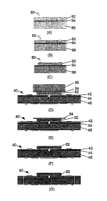
[0018] FIG. 5 is a schematic side view sho-wing zt process of n-ianufacturing
a structure
according to one preferred embodiment of the present invention;
[0019] FIG. 6 is a schematic side view showing a process of manufacturing a
MEMS
device together with bonding the MEMS device to the interposer wafer according
to
another preferred embodiment of the present invention;
10020] FIG. 7 is a schematic side view showing a process of manufacturing a
MEMS
device together with an interposer wafer according to another preferred
embodiment of the
present invention; and
[0021] FIG. 8 is a schematic side view of a wafer scale assembly that is used
to form an
array of MEMS devices according to one aspect of the present invention.
5b
CA 02573907 2007-01-15
WO 2006/019761
PCT/US2005/024763
tETAILE I DESCRIPTI IN OF PREFERRED EM IIIYEENTS
[0022] The present invention provides a configuration for a MEMS device, which
has a
silicon MEMS device directly bonded to an interposer wafer without the
intermediate
substrate and the brazing materials.
[0023] According to one preferred embodiment of the present invention, the
process is
based on a Bonded and Etch Back Silicon-On-Insulator (referred to hereinbelow
as
BESOT) method. BESOI is a fabrication method for producing MEMS and related
devices using Silicon-On-Insulator (SOT) materials. The method includes
providing a
Silicon-On-Insulator (SOT) wafer, which has (i) a handle layer, (ii) a
dielectric layer,
which preferably is a silicon dioxide, on the handle layer (Si02) layer, and
(iii) a device
layer on the dielectric layer. The device layer is first patterned by mesa
etch. After the
device layer is patterned, the SOT wafer is bonded to a substrate with the
patterned device
layer facing the substrate. The handle layer and the dielectric layer of the
SOI wafer are
then removed by etching. The device layer is further etched to define the MEMS
device.
In the BESOI method, the structure etching is performed after the dielectric
Si02 layer is
removed. One of the advantages of the BESOI process is that the SiO2 layer
functions as
an etching stop when the handle layer is removed by wet or dry etching, thus
preventing
the underneath device layer from being damaged by the etchant.
[0024] FIGS. 3 and 4 illustrate a process of manufacturing the MEMS device and
the
interposer according to the present disclosure. Those figures schematically
show side
views of the wafers in each fabrication step. The illustrated side views do
not represent
the whole structure of the wafer. For example, the number of ohmic contacts on
the
device layer of the wafer may not be limited to two. There may be more
contacts or
more other devices deposited on the wafer, that are not shown in FIGS. 3 and
4.
[0025] FIG. 3 illustrates a process of fabricating a wafer that will be used
to form the
interposer according to one aspect of the present invention. As shown in FIG.
3, the
process starts from (A) at the top of the figure and continues to (E) at the
bottom of the
figure. The process starts from constructing an interposer with an SOT wafer
40. As
shown in (A), the SOT wafer includes a device silicon layer 42, a dielectric
layer 44,
which preferably is a silicon dioxide (SiO2) layer, and a handle silicon layer
46. The
6
CA 02573907 2007-01-15
WO 2006/019761
PCT/US2005/024763
device layer 42 preferably is heavily doped, so that it is sufficiently
conductive. In an
alternate embodiment, the handle layer 46 may be heavily doped. The dopant
type and
concentration can be customized based on a user's need. Such SOT wafers are
commercially available in the market.
[0026] A thin oxide layer 48, preferably about 11.1m thick, is grown on a
bottom side of
the handle layer 46, as shown in (B). The thin oxide layer 48 is etched
defining holes
through the thin oxide layer 48 and ohmic contacts 52 are deposited at the
hole areas.
More ohmic contacts 50 are deposited on the top of the device layer 42, as
shown in (C).
The ohmic contacts 50 and 52 are preferably formed by metal, exemplary metals
including Al, Ti, Pt, and Au. Conventional metallization processes such as
physical
vapor deposition (PVD) and chemical vapor deposition (CVD) can be used for
depositing
the metal to form the contacts. Preferably, the contacts 50 and 52 are formed
by sputter
deposition. In next step, as shown in (D), heaters 54 and sensor 56 are formed
at the
bottom surface of the thin oxide layer 48. Preferably the heaters 54 are
formed by sputter
deposition of Ti and Pt, and the sensor 56 is formed by sputter deposition of
Ti, Pt, and
Au. The contacts 50, 52, the heaters 54, and the sensor 56 can be formed by
one or more
metal layers as listed above, or other electrically conductive materials, such
as highly
doped polycrystalline silicon. In next step, as shown in (E), the device layer
42 of the
wafer 40 is patterned to define electrically conductive areas. In the
exemplary
embodiment in (E), a deep trench 60 is formed through the device layer 42 and
the oxide
layer 44, separating the device layer 42 to two active areas, which are not
electrically
conductive with each other. In one preferred embodiment, in forming the trench
60, a
highly anisotropic etch, for example a Bosch etch, a reactive ion etch (RIE),
or an
inductively coupled plasma (ICP) etch, preferably performed in a Surface
Technology
Systems (STS) tool, is used to etch through the device silicon layer 42 to the
oxide layer
44. Then a reactive ion etching (RIB) or other suitable etch process is used
to etch
through the oxide layer 44. In RIB, a high selectivity of Si02 over silicon
can be obtained
by choosing the proper etch chemistry. The device layer 42 of the wafer 40 may
be
further patterned and metallized to form interconnect lines for connecting the
ohmic
contacts.
7
CA 02573907 2007-01-15
WO 2006/019761
PCT/US2005/024763
[0027] FIG. 4 illustrates a process of forming a MEMS device, followed by
bonding the
MEMS device to the interposer wafer 40, which has been formed in the process
in FIG.
3. The device forming and bonding-to-interposer process starts from (A) at the
top of
FIG. 4 and continues to (G) at the bottom of the figure. The process starts by
obtaining
or providing an SOI wafer 80, which is used to form the MEMS device. The SOI
wafer
80 includes a device silicon layer 82, a dielectric layer 84, which preferably
is a silicon
dioxide (Si02) layer, and a handle silicon layer 86. The device layer 82 may
be doped as
required by the MEMS device that the wafer 80 is to form. As shown in (B), an
etch is
performed on the device layer 82 to at least partially define the MEMS device.
In the
exemplary embodiment shown in FIG. 4, a mesa etch is performed to define
structural
posts 88. Preferably, one or more posts 88 are defined on the device layer 82.
In the next
step, as shown in (C), the wafer 80 is mounted to the wafer 40 by bonding the
top surface
of the posts 88 to the top surface of the device silicon layer 42 of the wafer
40. The
bonding technology will be presented in more detail below. In (C), after the
two wafers
80 and 40 are bonded together, the handle layer 86 of the wafer 80 becomes the
top layer
of the device. From (C) to (D) in FIG. 4, the top handle layer 86 is etched
away
preferably by a liquid etch, which stops on the upper surface of the oxide
layer 84, thus
protecting the underneath device silicon layer 82 from being damaged by the
etchant.
From (D) to (E), the oxide layer 84 is removed by a wet or dry etch, or a
combination of
wet and dry etch. The etchant used to remove the oxide layer 84 preferably has
a high
selectivity of Si02 over silicon, so that the underneath silicon will not be
attacked. From
step (E) to (F), the device layer 82 of the wafer 80 is further patterned to
define the
MEMS device. In a preferred form, an inductively coupled plasma (ICP) etching
performed in a Surface Technology Systems (STS) tool is used to define the
MEMS
device on the device layer 82. By way of example, the MEMS device can be used
to
form a gyroscope or an accelerator device. Other MEMS devices may also be
formed. In
the exemplary gyroscope and accelerometer embodiments, the device layer 82 is
etched
to define a proof mass as shown in (F). In step (G), the bottom wafer 40 is
further etched
preferably by inductively coupled plasma (ICP) to define the structure of the
interposer
and/or to separate the individual device from the wafer.
8
CA 02573907 2007-01-15
WO 2006/019761
PCT/US2005/024763
[0023] The device fabricated by the process described above has the MEMS
device 80
and the interposer 40 bonded by silicon direct bond, without brazing materials
or a
substrate layer between the top layer 82 of MEMS device 80 and the top layer
42 of the
interposer 40 as required in the prior art device for bonding the MEMS device
to the
interposer. The device fabricated by the process of the present disclosure has
better
stability and reliability over the lifetime of the device. Furthermore, the
present process
results in the MEMS device being directly bonded to the interposer without
using an
intermediate substrate, thus reducing the thermal mass of the MEMS device and
increasing the thermal stability of the combined interposer and MEMS
structure. The
number of processing steps to create the combined interposer and the MEMS
structure is
less than the number of steps needed to manufacture both items separately, and
then bond
them together.
[0029] It is preferred that the MEMS device 80 is bonded to the interposer 40
by silicon
direct bonding. Direct bonding, which is also called silicon fusion bonding,
is a wafer-
to-wafer bonding technology known in the art. The process includes three basic
steps:
surface preparation, contacting, and annealing. The surfaces that will be
bonded together
must be flat and smooth. The wafers to be bonded each should have a total
thickness
variation (TTV) less than 3 gm, and preferably less than lgm. The wafer
surfaces are
cleaned and processed in a clean room to form two hydrated surfaces. After
surface
preparation, the two wafers are contacted in a clean environment by pressing
the two
cleaned surfaces together. The next step is an elevated temperature anneal of
the
contacted wafers, preferably at a high temperature between 800 C to 1200 C.
Alternatively, the contacted wafers can be annealed at a lower temperature,
preferably
over a long time period. The bond strength at the interface between two wafers
can be
measured by various techniques, for example, a tensile/shear test. The bonding
method
that can be used to bond the two wafers is not limited to direct bonding.
Alternatives to
direct bonding include but are not limited to anodic bonding, intermediate-
layer
bonding, and the like. A wide range of intermediate layers and bonding
techniques can
be used in intermediate-layer bonding, for example, eutectic bonding using Au
thin films,
9
CA 02573907 2007-01-15
WO 2006/019761
PCT/US2005/024763
solder bonding, polymer bonding, low melting temperature glasses bonding, and
thermocompression bonding.
[0030] In the step when the top device silicon layer 82 is etched to define
the MEMS
device (e.g. the proof mass in gyroscope, accelerometer, or other devices), as
shown from
(E) to (F) in FIG. 4, the interposer 40, especially the contacts 50 on the top
surface of the
interposer 40, may be damaged during the etching process if without
protection.
Therefore, in another preferred embodiment, as shown in FIG. 5, a layer of
resist 90 is
deposited on the top surface of the device layer 82 at the areas above the
contacts 50 or
other devices on the interposer 40. The resist 90 can be the same resist that
is deposited
on the top surface of device layer 82 during the process of defining the MEMS
device, in
other words, after the oxide layer 84 is removed, a layer of resist 90 is
deposited on the
surface of the device layer 82, and in a following photolithography process,
the resist 90
is patterned for etching the device layer 82 to define the MEMS device and
also to
protect the underneath contacts 50 and other devices on the top of interposer
40. FIG. 5
shows a schematic view of the wafer 80 after the resist 90 is patterned by the
photolithography process. As seen from the figure, in the following etching
process,
preferably an inductively coupled plasma (ICP) etching, the contacts 50 on the
interposer
40 are protected from being etched by the plasma.
[0031] FIG. 6 illustrates another process that can be used to manufacture the
MEMS
device. The whole process also includes providing an interposer, which is the
same as
shown in FIG. 3, and manufacturing a MEMS device together with bonding the
MEMS
device to the interposer. The process of manufacturing a MEMS device together
with
bonding the MEMS device to the interposer starts from step (A) at the top of
the figure
and continues to step (G) at the bottom of the figure. At step (A), a standard
SOI wafer
80 is provided, which includes a device silicon layer 82, a dielectric layer
84, which
preferably is a silicon dioxide (Si02) layer, and a handle silicon layer 86.
The device
layer 82 has a thickness and conductivity of the MEMS device (i.e. the proof
mass) that
will be formed. In step (B), a mesa etch is performed on the device layer 82
to at least
partially define the structure of the MEMS device. In the exemplary
embodiment,
structural posts 88 are defined on the device layer 82. In the next step, as
shown in (C),
CA 02573907 2007-01-15
WO 2006/019761
PCT/US2005/024763
an inductively coupled plasma (ICP) etch is performed, preferably in an STS
tool, on the
device silicon layer 82 to further defme the MEMS device. The etch is
performed
through the device layer 82 and stops at the underlying oxide layer 84. In
next step, as
shown in (D), the wafer 80 is bonded to the interposer wafer 40. The
interposer wafer 40
has been prepared in a previous manufacturing process as shown in FIG. 3. The
posts 88
are bonded to the top surface of the device layer 42 of the wafer 40
preferably by direct
bonding as described above. From (D) to (E), the handle layer 86 is etched
away
preferably by a liquid etch, which stops on the upper surface of the oxide
layer 84, thus
protecting the underneath device silicon layer 82 from being damaged by the
etchant.
From (E) to (F), the oxide layer 84 is removed by a wet or dry etch, or a
combination of
wet and dry etch. The etchant used to remove the oxide layer 84 preferably has
a high
selectivity of Si02 over silicon, so that the underneath silicon will not be
attacked. In
step (G), the bottom interposer wafer 40 is further etched preferably by
inductively
coupled plasma (ICP) to define the structure of the interposer and/or to
separate the
individual device from the wafer. The device is then ready to be mounted in a
package.
[0032] This device also does not have the brazing materials or an intermediate
substrate
layer between the top layer MEMS device and the interposer as required in the
prior art
device for bonding the MEMS device to the interposer, and therefore, the
performance of
the device is improved.
[0033] In the embodiments shown in FIGS. 4-6, the structural posts 88 are
defined on the
wafer that is used to form the MEMS device. Alternatively, the structural
posts 88 can
be defined on the interposer wafer 40. This alternative process, as
illustrated in (A) in
FIG. 7, starts using an SOT wafer 40 that is used to form the interposer. As
shown in (B),
a mesa etch is performed on the device layer 42 of the interposer wafer 40 to
define
structural posts 88. Then, similar to the process illustrated in FIG. 3, a
thin oxide layer is
formed at a bottom surface of the interposer wafer 40, one or more ohmic
contacts,
sensors, and one or more heaters are formed on the interposer wafer 40, and a
trench is
defined through the device layer 42 and the oxide layer 44 of the interposer
wafer 40. As
shown in (D), another SOT wafer 80, which is used to form the MEMS device, is
bonded
to the interposer wafer 40 with the device layer 82 of the wafer 80 facing the
posts 88.
11
CA 02573907 2007-01-15
WO 2006/019761
PCT/US2005/024763
From (D) to (E), after the two wafers are bonded together, the handle layer 86
of the
MEMS device wafer 80 is removed by etching. From (E) to (F), the oxide layer
84 of the
MEMS device wafer 80 is removed by etching. From (F) to (G), the device layer
82 of
the MEMS device wafer 80 is further etched to define the MEMS device. In step
(H), the
bottom wafer 40 is further etched to define the structure of the interposer
and/or to
separate the individual device from the wafer 40.
[0034] The present disclosure has described MEMS devices and methods for
producing
the MEMS devices in a single device level. Such devices are typically
fabricated in large
numbers on a wafer of semiconductor material. The wafer scale assembly is then
separated into individual devices. A person skilled in the art should
appreciate that the
wafer scale fabrication uses the same process as described in the
specification and as
claimed in the claims.
[0035] FIG. 8 schematically illustrates a wafer scale assembly 100 (the figure
shows part
of the assembly), which includes two wafers bonded together, an SOT wafer 40
which is
used to form the interposers and an SOT wafer 80 which is used to form the
MEMS
devices. The wafer scale assembly includes an array of structures 102 that are
used to
form an array of MEMS devices. The etching process of the MEMS devices in
wafer
scale is the same as the process described in the above paragraphs and
illustrated in the
figures. After the wafer scale assembly 100 is etched, an array of the MEMS
devices are
defined on the interposer wafer 40. The result structure is then separated
into individual
MEMS devices.
100361 A person skilled in the art should understand that the processes
described above
and in the figures only briefly illustrate the fabrication processes, and some
detailed steps
are not described in the description and in the figures, for example, in any
etching step,
the steps of deposition of photoresist and photolithography not described in
the
description and figures. One skilled in the art should understand that these
steps are
required in the fabrication process and should appreciate the whole
fabrication process
from the exemplary embodiments illustrated in the present disclosure. The
specification
describes the steps of the preferred processes in a sequence, but a person
skilled in the art
12
CA 02573907 2007-01-15
WO 2006/019761
PCT/US2005/024763
should understand that it may not be necessary to perfonn these steps in the
sequence as
described, for example, step (G) in FIGS .4 and 6 may be performed in an
earlier stage.
[0037] The invention may be embodied in other specific forms without departing
from
the spirit or essential characteristics thereof The present embodiments are
therefore to be
considered in all respects as illustrative and not restrictive, the scope of
the invention
being indicated by the appended claims rather than by the foregoing
description, and all
changes which come within the meaning and range of equivalency of the claims
are
therefore intended to be embraced therein.
13