Note : Les descriptions sont présentées dans la langue officielle dans laquelle elles ont été soumises.
CA 02579325 2007-02-20
BACKGROUND OF THE INVENTION
1. Field of the Invention
The invention relates to a method for producing a
semiconductor component having a metallic control electrode, and to
a semiconductor component having a metallic control electrode. The
metallic control electrode as a gate electrode of a field effect
transistor has a narrower gate foot, and a broader gate head, and
is typically approximately T-shaped.
2. The Prior Art
In the case of monolithically integrated circuits having
field effect transistors, particularly HEMT high-performance field
effect transistors, the gate length of the gate as a control
electrode is of particular importance. The precise production of
very small gate lengths below 300 nm is critical. The material
combination of metal of the control electrode and of the
semiconductor material is of essential significance on the basis of
alloy formation, diffusion, chemical reaction and influence on the
semiconductor properties. Frequently, electrode metals that are
suitable on Si substrates are not suitable for compound
semiconductor materials, particularly GaAs and InP, and vice versa.
Particularly in the case of components on a GaAs
substrate, aluminum is advantageous as a gate material, as compared
with Ti/Pt/Au control electrodes that are frequently used.
Aluminum possesses particularly great conductivity and forms a
connection with the semiconductor material that is particularly
stable in the long term, without impairing the properties of the
material by means of diffusion.
- 1-
CA 02579325 2007-02-20
A control electrode made of aluminum is described in
German Patent No. DE 103 04 722 Al, in which aluminum is deposited
over the entire area and the gate head is produced by means of
subsequent marking and etching from the continuous metal layer. In
another lift-off technique that is frequently used, a structure for
a gate head is predetermined in a mask. It is advantageous if the
gate foot and the gate head are aligned with one another in a self-
adjusting manner.
After deposition of the gate metal, at least one
temperature treatment at elevated temperature is required.
However, it has been shown that with decreasing gate length, the
field effect transistors having an Al gate tend to exhibit NOPO (NO
Pinch Off) errors, making the components unusable for many
applications.
SUMMARY OF THE INVENTION
It is therefore an object of the present invention to
provide a method for producing a semiconductor component and a
semiconductor element on a III-V compound semiconductor substrate,
which possesses advantageous properties, and is stable in the long
term, even at a small gate length.
This object is achieved according to the invention by a
method for producing a semiconductor component having a metallic
gate electrode deposited onto a semiconductor layer, with a gate
foot and a gate head. After deposition of the metal of the gate
electrode, a temperature treatment at elevated temperature is
carried out, and a first layer (G1) of the gate electrode, of
- 2-
CD, 02579325 2007-02-20
aluminum, is produced on the semiconductor layer, a second layer
(G2) of a second metal is deposited on the first layer (G1), which
metal limits the growth of the grain sizes of the aluminum in the
first layer (G1) during the subsequent heat treatment, and
additional metal, different from the second metal, is deposited on
the second layer in at least one additional layer (G3).
In the case of the invention, the advantageous properties
of the contact between aluminum (Al) as the material of a first
layer of the gate foot, and the compound semiconductor material of
the semiconductor layer, particularly on GaAs substrate, are
maintained. In this connection, unless indicated otherwise, the
semiconductor layer is that semiconductor layer on which the
control electrode is structured and disposed. The control
electrode can, in particular, form a Schottky diode with the
semiconductor layer. By means of inserting a second layer of a
different metal, it is advantageously possible to avoid the NOPO
errors even at very small gate lengths, and to achieve advantageous
properties of the field effect transistor that are stable in the
long term.
The invention takes advantage of the recognition that an
essential reason for the occurrence of the stated NOPO errors is a
grain size growth of the aluminum that occurs during the
temperature treatment and/or in operation, due to electromigration.
A larger grain size in aluminum as the gate metal is actually
advantageous for low electrical resistance of the gate control
electrode. However, it has been shown that with a decreasing gate
length, a larger grain size has a disadvantageous effect in the
narrow gate foot.
- 3-
CA 02579325 2007-02-20
This disadvantageous phenomenon is counteracted,
according to the invention, in that aluminum, with its advantageous
physical properties, is used as the gate metal in a thin, first
layer, having a first layer thickness, and the grain size growth in
the first layer is limited to smaller average grain sizes than in
the case of a gate consisting entirely of aluminum, by means of a
second layer of a second metal, different from aluminum.
For the second layer, it is advantageous if a metal is
selected that can be alloyed with the aluminum of the first layer,
and is alloyed with the Al of the first layer at the layer border
between the first and second layer, during a temperature treatment
that is carried out after deposition of the metal of the gate
electrode, preferably at approximately 400 C. It is advantageous
if the alloy layer that results from this is at a sufficient
distance from the semiconductor layer to avoid impairments of the
properties of the metal-semiconductor transition.
It is advantageous if platinum (Pt), nickel (Ni), or
preferably titanium (Ti) is deposited onto the first layer as the
second metal in the second layer. It is advantageous if the second
layer thickness is less than 10 nm, particularly less than 5 nm,
preferably less than 2.5 nm.
It is advantageous if additional gate metal that is
different from the metal of the second layer is deposited in at
least one additional layer. It is advantageous if the gate head
consists at least predominantly of the additional metal. The
additional metal is preferably deposited in a layer thickness that
- 4-
CA 02579325 2007-02-20
is greater than the sum of the first and second layer thickness.
It is advantageous if aluminum is used as the additional
metal. This prevents the other metal from diffusing from the
additional layer through the thin second layer, in the direction of
the first layer and the semiconductor layer, and thereby prevents a
detrimental influence on the component properties. It is
advantageous if the average grain size of the aluminum in the first
layer, after the temperature treatment, is smaller than in the
additional layer, and preferably amounts to less than 50%,
particularly less than 20% of the average grain size in the
additional layer.
The deposition of the gate metal preferably takes place
by means of vapor deposition. It is advantageous if the
structuring of the gate head takes place in a self-adjusting manner
relative to the gate foot. The greatest expanse of the gate head
in the direction of the gate length preferably amounts to at least
1.5 times the gate length, and can typically amount to as much as
approximately 600 nm. It is advantageous if the greatest expanse
of the gate head in the direction of the gate length is at least
100 nm greater than the gate length. The gate length can be
reduced to as much as approximately 20 nm.
It is advantageous if the gate foot is deposited in a
recess channel of the semiconductor surface, for which purpose an
opening having the structure of the gate and lateral under-etching
is produced in a layer deposited on the semiconductor material. It
is advantageous if the layer thickness of the first layer amounts
to at least 50%, particularly at least 65%, preferably at least 75%
- 5-
ak 02579325 2014-04-17
of the depth of the recess channel, thereby making it possible
to prevent or limit disadvantageous effects, particularly when
using Ti as the second metal, caused by different vapor
deposition behavior of the Ti.
In accordance with an aspect of the present disclosure
there is provided a semiconductor component having a metallic
gate electrode on a semiconductor layer of semiconductor
material on GaAs substrate, said gate electrode having a gate
foot and a gate head and consisting of several layers when
viewed in a direction perpendicular to a plane of the
semiconductor layer, said layers comprising: a first layer (G1)
consisting of aluminum and having a first layer thickness (D1);
a second layer (G2) on top of the first layer (G1) and
consisting of a second metal, different from aluminum; and at
least one additional layer (G3) formed above the second layer
and consisting of an additional metal, different from the metal
of the second layer, wherein the additional layer comprises
aluminum, and wherein an average grain size of the aluminum in
the first layer is less than an average grain size of the
aluminum in the additional layer.
BRIEF DESCRIPTION OF THE DRAWINGS
Other objects and features of the present invention will
become apparent from the following detailed description
considered in connection with the accompanying drawings. It is
to be understood, however, that the drawings are designed as an
illustration only and not as a definition of the limits of the
invention.
-6-
CA 02579325 2014-04-17
In the drawings, wherein similar reference characters
denote similar elements throughout the several views:
FIGS. la-id show a process sequence according to the
invention, in several steps; and
FIG. 2 shows an enlarged detail from FIG. ld.
DETAILED DESCRIPTION OF THE PREFERRED EMBODIMENT
Referring now in detail to the drawings, different process
stages for the production of a control electrode are sketched in
FIG. la to id. Proceeding from a GaAs substrate 1, layers 2 to 5
form the vertical profile of a field effect transistor. A great
number of examples are known for the layer
-6a-
CD, 02579325 2007-02-20
sequence, from the state of the art. The number of layers, the
layer thickness values, and the composition of the materials can
vary in an individual case.
Typically, layer 2 represents a buffer layer, layer 3
forms a semiconductor layer with the two-dimensional electron gas
(the channel), layer 4 is a barrier layer and forms the
semiconductor layer on which the metal of the control electrode is
deposited, and which forms a Schottky diode with the control
electrode, and layer 5 is a highly doped contact layer for low-ohm
resistive component contacting by way of ohmic contacts OC. Layer
4, in particular, can have a stop layer as an etch stop for etching
processes during the course of production of the component, in its
layer border that lies on top, i.e. facing away from the substrate.
Layer 5 preferably consists of GaAs and, if applicable,
additional stop layers consist of AlAs or InGaP, for example.
After production of layer sequence 2 to 5 on substrate 1,
and production of the ohmic contacts OC, a protective layer 6, for
example made of silicon dioxide and/or silicon nitride, is
deposited over the whole area.
A layer of photoresist or similar material is deposited
on protective layer 6, and the gate structure is produced in it by
way of photolithography. With structured layer 7 as a mask, an
opening MF is produced in protective layer 6, which opening
determines the structure of the gate foot. An opening MK in
photoresist layer 7 determines the structure of the gate head of
the control electrode. Opening MF in protective layer 6 and
- 7-
CD, 02579325 2007-02-20
opening MK in photoresist layer 7 can be produced by means of
separate photolithography steps, or with only a single
photolithography step, in self-adjusting manner. The recess
channel RC that extends on both sides of the opening MF is produced
by means of opening MF in protective layer 6, with lateral under-
etching of protective layer 6 into contact layer 5. In this
connection, the depth of the recess channel corresponds to the
layer thickness of contact layer 5. The gate metal is deposited
onto barrier layer 4 by means of cathode sputtering or preferably
by means of vapor deposition, through opening MF, and onto
protective layer 6 through opening MK, whereby an approximately T-
shaped electrode having a narrower gate foot and a broader gate
head is formed. The deposited gate metal is also deposited onto
the photoresist layer in the surroundings of the gate head, and can
be removed from there in a lift-off method, in advantageous manner.
The method described up to this point is fundamentally known from
the state of the art, in a great number of variants. Instead of
the lift-off method, structuring of the gate head from a continuous
metal layer by means of etching can also be performed, as is also
known from the prior art cited in the introduction to the
specification.
In the case of deposition of the gate metal according to
a preferred embodiment of the present invention, a first layer G1
of Al, on this a second layer G2 of Pt, Ni, or preferably Ti, and
then again, another layer G3 of Al on this are deposited, one after
the other. In the case of structuring of the gate head by means of
etching a continuous metal layer, Ti is also preferred because of
its better etchability.
- 8-
CA 02579325 2007-02-20
After complete deposition of the gate metal according to
Fig. la, the metal deposited on the photoresist layer 7 is removed
by means of lift-off with dissolution of the latter, and the
structure according to Fig. lb is formed. In this situation, a
first temperature treatment at elevated temperature, for example at
approximately 400 C, is typically carried out. Within the
framework of this temperature treatment, grain size growth of the
aluminum occurs in layers G1 and G3. The grain size growth in the
layer G1 is limited to smaller grain sizes than in the layer G3,
because of the measures taken according to the present invention,
particularly the restriction of the layer thickness D1 (Fig. 2) of
the layer Gl.
Afterwards, the protective layer 6 is removed, and the
component structure exposed in Fig. lc is coated with a passivation
layer 8 according to Fig. ld. The application of this passivation
layer to a component surface is known.
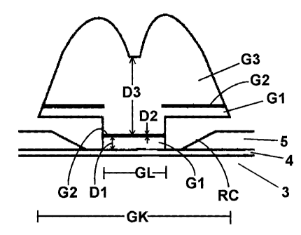
The present invention essentially relates to the layer
structure of the metallic gate electrode of a first layer G1 on the
semiconductor material of the semiconductor layer 4 in the recess
channel RC, a second layer G2 on the first layer, and another layer
G3 on the second layer G2, as shown in the example. The layer
sequence is found both in the gate foot above the semiconductor
material in the recess channel, and in the gate head above the
protective layer to the side of the opening MF. The proportions of
the individual layers and/or the control electrode in the figures
are not to be understood as being strictly to scale.
- 9-
CA 02579325 2007-02-20
The layer G1 consists of aluminum, which forms a boundary
surface to the material of the semiconductor layer 4, in
particularly advantageous manner, and can form a Schottky diode
with it, in particular. The layer 1 is deposited at a layer
thickness D1, which is advantageously not greater than 1.5 times
the gate length GL, particularly not greater than the gate length
GL of the control electrode, see Fig. 2. The layer G1 is also
found to the side of the opening MF and within the opening MK on
the upper surface of the protective layer 6, with a width GK of the
gate head parallel to the direction of the gate length.
It is advantageous if the gate length GL lies below 300
nm, particularly in a range between 20 nm and 300 nm. The width GK
of the gate head is greater than the gate length GL and preferably
amounts to at least 1.5 times the gate length GL. It is
advantageous if the width GK of the gate head lies between 400 nm
and 650 nm.
The thickness D1 of the first layer G1 perpendicular to
the plane of the semiconductor layer advantageously lies between 10
nm and 100 nm. Particularly with the preferred use of Ti as the
metal of a second layer deposited on the first layer, the layer
thickness D1 of the first layer advantageously amounts to at least
50%, particularly at least 65%, preferably at least 75% of the
depth of the recess channel RC under the protective layer 6. The
depth of the recess channel is at least approximately equal to the
layer thickness of the contact layer 5. Penetration of Ti, vapor-
deposited with great divergence, into the recess channel is avoided
or can be kept low by means of a slight distance between the upper
layer border of the first layer and the opening MF in the
- 10-
CA 02579325 2007-02-20
protective layer 6. The first layer can also reach all the way
into the opening MF.
A second layer G2 of a second metal (or metal mixture) is
deposited onto the first layer G1 through the opening MF and
through the opening MK. The second metal is different from
aluminum and advantageously possesses the property of being able to
form an alloy with aluminum, and of limiting the grain size growth
of aluminum in the layer Gl, during subsequent heat treatment or
due to electromigration during operation. Pt, Ni, or, in
particular, Ti are suitable, for example. A restriction of the
grain size growth occurs, in particular, due to the fact that
grains in the aluminum layer G1 grow in all directions at the same
time, and that a stop in the grain size growth at the layer border
from G1 to G2 essentially brings about a stop in the grain size
growth transverse to the layer border plane. Therefore, a low
layer thickness of the layer G1 is of particular significance.
The second layer thickness D2 of the second layer G2 is
advantageously less than 10 nm, particularly less than 5 nm,
preferably less than 2.5 nm. Additional gate metal in at least one
additional layer, preferably precisely one additional layer G3 is
deposited on the second layer G2. The deposition of the additional
gate metal in the layer G3 takes place in a layer thickness D3 that
is advantageously greater than the sum of the first layer thickness
and second layer thickness, G1 and G2. It is advantageous if the
gate head consists predominantly of the additional gate metal in
the additional layer G3.
It is advantageous if the additional layer G3 consists of
- 11-
ak 02579325 2007-02-20
aluminum as the additional gate metal. This advantageously has a
very low specific electrical resistance.
Grain size growth occurs also in the aluminum of the
additional layer G3 as a result of the subsequent temperature
treatment, advantageously at about 400 C, and/or during operation
of the component, due to electromigration. Here, however, no
measures are required or provided to limit the grain size growth.
Larger grain sizes can be advantageous with regard to the
electrical resistance of the gate thread, which stands
perpendicular to the plane of the drawing. It is advantageous that
after the temperature treatment, an average grain size of the
aluminum occurs in the first layer G1 that is less than the average
grain size of the aluminum in the additional layer G3, and
advantageously less than 50%, particularly less than 20% of the
average grain size of the aluminum in the additional layer G3.
During the temperature treatment, alloy formation of the
various metals also occurs at the border surfaces of the second
layer G2 to the first layer G1 and the third layer G3. An alloy
zone that forms in the first layer advantageously does not reach
all the way to the semiconductor layer 4, and is at a sufficient
distance from layer 4, so that the properties of the Schottky
transition between the first layer G1 of the control electrode and
the semiconductor layer 4 are not impaired by the alloy.
The characteristics indicated above and in the claims as
well as evident from the figures can be advantageously implemented
both individually and in various combinations. The invention is
not limited to the exemplary embodiments described, but rather can
- 12-
CA 02579325 2014-04-17
be modified in many different ways, within the scope of the
abilities of a person skilled in the art. In particular, with
regard to the composition of the semiconductor layers, different
variants are familiar to a person skilled in the art as being
equivalent, and, in particular, an InP substrate can also be
provided instead of a GaAs substrate.
The scope of the claims should not be limited by the preferred
embodiments set forth in the examples, but should be given the
broadest interpretation consistent with the description as a
whole.
- 13 -