Note : Les descriptions sont présentées dans la langue officielle dans laquelle elles ont été soumises.
CA 02579828 2007-02-23
Doc. No. 102-26 CA
Patent
METHOD OF CHANGING THE REFRACTIVE INDEX IN A REGION OF A CORE
OF A PHOTONIC CRYSTAL FIBER USING A LASER
FIELD OF THE INVENTION
This invention relates generally to the direct writing of gratings in photonic
crystal structures
such as microstructured optical fiber and photonic crystal waveguides using a
diffraction
grating and femtosecond pulsed light; and, one aspect of this invention
relates to the
modification of microstructured optical fiber or waveguides to facilitate the
inscription of
gratings therein.
BACKGROUND OF THE INVENTION
Optical fibers are used in many fields including telecommunications, laser
machining and
welding, laser beam and power delivery, fiber lasers, sensors and medical
diagnostics and
surgery. They are typically made entirely from solid transparent materials
such as glass and
each fiber typically has the same cross-sectional structure along its length.
The transparent
material in one part (usually the middle) of the cross-section has a higher
refractive index than
the rest and forms an optical core Within which light is guided by total
internal reflection. We
refer to such a fiber as a standard fiber.
Although the light is confined to the core in a standard fiber, the cladding
plays an active part
in the wave-guiding process because a guided mode will extend some distance
into the
cladding. The cladding is also important for a relatively new class of fiber
devices, know as
cladding-pumped fiber lasers and amplifiers. The fibers used in such devices
have an inner
core, in which signal light propagates as a single-mode, and which is doped
with some active
material, typically a rare earth element. The inner core is nested in a larger
outer core, which is
multimode at both signal and pump wavelengths. Typically, the inner core is
nested off-center
within the outer core, to improve the overlap between the core mode and the
modes of the
cladding. High-power multi-mode pump light can be introduced into the outer
core with a
high efficiency, and propagates down the fiber, being gradually absorbed by
the rare earth
1
CA 02579828 2007-02-23
Doc. No. 102-26 CA
Patent
element present in the inner core. The signal in the inner core is then
amplified, forming an
optical amplifier or, with appropriate feedback, a laser.
Evanescent fiber sensors and couplers based on standard fibers are known in
the form of "D"
fibers. The preform from which a "D" fiber is drawn is polished away on one
side until the
core is close to the surface of the fiber. The fiber is then drawn and the
thin layer of cladding
glass remaining adjacent to the core in the previously polished region is
etched away over a
short length of fiber. The evanescent field of light propagating in the fiber
is thus readily
accessible only over that short length.
In the last few years, a non-standard type of optical fiber has been
demonstrated, called the
photonic-crystal fiber (PCF). Typically, this is made from a single solid, and
substantially
transparent, material within which is embedded a periodic array of air holes,
running parallel
to the fiber axis and extending longitudinally, the full length of the fiber.
A defect in the form
of a single missing air hole within the regular array forms a region of raised
refractive index
within which light is guided, in a manner analogous to total-internal-
reflection guiding in
standard fibers. The effective refractive index of each region of the fiber
may be calculated
using the methods outlined in, fonexample, Birks et al, Opt. Lett 22 961
(1997). Another
mechanism for guiding light is based on photonic-band-gap effects rather than
total internal
reflection. Photonic-band-gap guidance can be obtained by suitable design of
the array of air
holes (see, for example, Birks et al, Electron. Lett. 31 1941 (1995)). Light
with particular
propagation constants can be confined to the core and will propagate therein.
Photonic-crystal fiber can be fabricated by stacking, on a macroscopic scale,
glass canes--
some of which are capillaries--into the required shape and then holding them
in place while
fusing them together and drawing them down into a fiber. PCF has unusual
properties such as
the ability to guide light in a single-mode over a very broad range of
wavelengths, and to
guide light having a relatively large mode area which remains single-mode.
2
CA 02579828 2007-02-23
Doc. No. 102-26 CA
Patent
This invention relates to the writing of Bragg gratings in the core of PCF and
the overcoming
of difficulties that have been associated therewith.
The fabrication of many photonic devices has been achieved through exposure of
transmissive
and absorbing materials to intense laser radiation in order to change the
optical properties of
said materials. For example, UV-induced photo-sensitivity of germanium doped
silica glasses
has been exploited in order to create permanent refractive index changes in
the photosensitive
Ge-doped silica cores of single mode optical fibers and waveguides as opposed
to the undoped
cladding. By creating a spatial intensity modulation of the UV exposure either
by using a two-
beam interference technique as disclosed in US patent #4,807,950 by Glenn et
al. or by using
a phase mask as disclosed in US patent #5,367,588 by Hill et al., Bragg
grating structures can
be produced in the photosensitive 'bore of the waveguide.
Bragg gratings in optical fiber and waveguides have developed into an
important technology
for wavelength division multiplexing (WDM) systems and other applications for
fiber optic
systems such as optical sensing because of the highly desirable optical
characteristics the
Bragg structures exhibit as well as the relative ease with which they can be
fabricated. A large
variety of optical devices have been fabricated using Bragg gratings in
waveguides including
optical add/drop multiplexing filters (OADM), gain flattening filters, band
splitters and
dispersion compensators.
Photonic crystal fibers (PCFs) or microstructured fibers, as described above,
consisting of a
periodic array of air holes that make up a cladding region about a solid core,
represent a new
class of waveguides with unique modal, dispersive and nonlinear properties
that have found
applications in a variety of optical fields. The coupling of these two
technologies, by the
fabrication of grating structures within PCFs, has received much attention
recently because of
the potential advantages of exploiting together the distinct strengths of each
technology.
Gratings fabricated in PCF with a Ge-doped core using existing FBG fabrication
techniques
are described by B. J. Eggleton et al. in "Grating resonances in air-silica
microstructured
3
CA 02579828 2007-02-23
Doc. No. 102-26 CA
Patent
optical fiber," Opt. Lett. 24, 1460 (1999). Modest strength gratings have also
been made in
standard all-silica PCF using phase masks and an ArF excimer and UV
femtosecond pulse
duration laser radiation.
Although these prior art Bragg gratings in photonic crystal fiber provide a
useful function,
they are known to suffer from some limitations in terms of the strength of the
grating
resonance that can be produced. In fact only modest refractive index
modulations have been
reported, i.e., ¨ 1 x 10⁴ and in the case of photonic crystal fiber consisting
of pure silica, the
grating writing times in this PCF were prohibitively long; over 1 hour when
high photonic
energy Argon Fluoride UV excimer laser radiation or high intensity femtosecond
UV radiation
is used.
Unfortunately, with side exposure inscription of Bragg gratings in PCF,
scattering of light by
the cladding holes is deleterious, especially when the exposure wavelength is
on the same
order as the hole dimensions and hole spacing or pitch that make up the
photonic crystal
cladding region, or more precisely the exposure wavelength is resonant with
the photonic
band gap created by the hole dimensions and spacing. The resulting intensity
of energy
incident on the core region is greatly reduced. PCFs have been characterized
and the band
gaps for particular PCFs have been determined. E. C Magi et al. in a paper
entitled
Transverse Characterization of Tapered Photonic Crystal Fibers, Journal of
Applied Physics
Vol 96 No. 7, 1 Oct 2004, disclose the characterization of PCF as a function
of a taper
diameter, and rotational orientation of the photonic crystal lattice of the
taper with respect to
the incident probe beam, however there is no suggestion of writing a structure
in such a fiber
as a function of a mismatch between the irradiating wavelength and the band
gap of the PCF.
As a solution to this problem we have discovered that this effect can be
mitigated by either
using a fiber geometry with fewer intervening holes between the core and outer
surface or by
removing or effectively removing the holes altogether. We have further
discovered that by
tapering a photonic crystal fiber sufficiently, scattering of light that
otherwise would have
occurred when writing a grating into the PCF using IR light can be lessened or
effectively
4
CA 02579828 2007-02-23
Doc. No. 102-26 CA
Patent
eliminated so that a high contrast grating can be written into the PCF. The
hole diameter and
hole spacing is reduced however in the absence of hole collapse; the ratio of
hole diameter to
hole spacing is constant. The change in hole diameter and spacing shifts the
photonic band
gap generated by the cladding holes away from the exposure wavelength.
Effectively
It is an object of this invention to overcome the aforementioned limitations
within the prior art
the incident radiation used for writing a grating in the core region of a
photonic crystal optical
fiber by changing an aspect of the PCF's response to the light by: injection
of index matching
fluid into the cladding holes of the photonic crystal fiber which is
transmissive to the radiation
but is index matched to the photonic crystal fiber material (typically
silica); or by tapering the
CA 02579828 2007-02-23
Doc. No. 102-26 CA
Patent
PCF suitably so as to narrow a portion of the fiber prior to irradiating the
fiber with light so as
to write a grating therein.
SUMMARY OF THE INVENTION
In accordance with this invention a method of writing a grating in a photonic
crystal
waveguide is provided comprising the steps of:
providing a PCF having a cladding surrounding a core;
b) changing an aspect of the PCF's response to incident light, so as to lessen
unwanted
scattering that would otherwise occur in the absence of changing said aspect
when irradiating
the PCF with the irradiation;
and irradiating the PCF from a side with laser light having an intensity I,
wavelength and
suitable duration so as to effect a refractive index change within the PCF of
at least lx 10-5
wherein at least (0.1)I of the light is transmitted through the cladding to
reach the core,
wherein I is greater than 102 W/cm2 and less than 5x10'3 W/cm2 for a silica
based PCF. To
inscribe a grating in hydrogen loaded standard fiber with continuous wave 244
nm (UV), an
intensity of ¨300 W/cm2 is required. This represents the lower intensity
limit. To inscribe a
grating with ultrafast IR without damaging SMF fiber, the peak intensity is
¨5x10¹³ W/cm2)
=
This invention provides a structure for allowing incident IR femtosecond
radiation to reach
the core area of a photonic crystal optical fiber, which would otherwise
normally be scattered
by holes that make up the cladding region of the photonic crystal fiber. If
the incident IR
radiation is modulated by a phase mask or is tightly focused then a Bragg
grating could be
written. This invention also provides a different structure which would allow
for increase UV
radiation to reach the core area. This can also apply to an instance where the
PCF core is
germanium doped and CW UV lasers are used for the inscription. Hydrogen loaded
germanium doped PCF may have end thereof fused so the hydrogen does not easily
escape,
prior to inscribing a grating.
6
CA 02579828 2007-02-23
Doc. No. 102-26 CA
Patent
In accordance with an embodiment of this invention, a method for inducing a
spatially
modulated refractive index pattern in a photonic crystal optical fiber or
waveguide is
provided, comprising the steps of:
providing the photonic crystal optical fiber or waveguide;
tapering the photonic crystal fiber such that the photonic band gap formed by
the presence of
the cladding holes is at least 10% transmissive to electromagnetic radiation
having a
predetermined wavelength range such that at least 10% of the electromagnetic
radiation can
reach the core;
disposing a mask to be used as an interferometer, adjacent the photonic
crystal optical fiber or
to waveguide such that light incident upon the mask is transmitted directly
into said optical fiber
or waveguide; and,
providing electromagnetic radiation on a surface of the mask, the
electromagnetic radiation
having a predetermined wavelength range and having a pulse duration of less
than or equal to
500 picoseconds, wherein the mask is disposed to permit a portion of the
electromagnetic
radiation to interact with the mask and be incident on the photonic crystal
optical fiber or
waveguide, the interaction of the electromagnetic radiation with the mask for
producing a
spatial intensity modulation pattern within the photonic crystal optical fiber
or waveguide, the
electromagnetic radiation incident on the photonic crystal optical fiber or
waveguide being
sufficiently intense to cause a change in an index of refraction of the
photonic crystal optical
fiber or waveguide, wherein electromagnetic radiation interacting with the
surface of the mask
having a sufficiently low intensity to not significantly alter produced
spatial intensity
modulation properties of the mask.
In accordance with another aspect of the invention, there is provided a method
of inducing a
spatially modulated refractive index pattern in a photonic crystal optical
fiber or waveguide,
comprising the steps of:
providing the photonic crystal optical fiber or waveguide;
tapering the photonic crystal fiber adiabatically such that the photonic
crystal optical fiber or
waveguide propagates in single mode electromagnetic radiation having a
predetermined
wavelength range and
7
CA 02579828 2007-02-23
=
Doc. No. 102-26 CA
Patent
collapsing the holes in the tapered region of said photonic crystal optical
fiber or waveguide
such that light propagating in the collapsed region fills the collapsed region
cross-section;
wherein the collapsed region is transmissive to electromagnetic radiation
having a
predetermined wavelength range (used to induce the index change)
disposing a mask to be used as an interferometer, adjacent the photonic
crystal optical fiber or
waveguide such that light incident upon the mask is transmitted directly into
said optical fiber
or waveguide; and,
providing electromagnetic radiation on a surface of the mask, the
electromagnetic radiation
having a predetermined wavelength range and having a pulse duration of less
than or equal to
500 picoseconds, wherein the mask is disposed to permit a portion of the
electromagnetic
radiation to interact with the mask and be incident on the photonic crystal
optical fiber or
waveguide, the interaction of the electromagnetic radiation with the mask for
producing a
spatial intensity modulation pattern within the photonic crystal optical fiber
or waveguide, the
electromagnetic radiation incident on the photonic crystal optical fiber or
waveguide being
sufficiently intense to cause a change in an index of refraction of the
photonic crystal optical
fiber or waveguide, wherein electromagnetic radiation interacting with the
surface of the mask
having a sufficiently low intensity to not significantly alter produced
spatial intensity
modulation properties of the mask.
In accordance with another aspect of the invention, there is provided a method
for inducing a
spatially modulated refractive index pattern in a photonic crystal optical
fiber or waveguide,
comprising the steps of:
providing the photonic crystal optical fiber or waveguide;
providing a fluid into the cladding holes of the photonic crystal fiber or
waveguide that is
substantially index matched to the refractive index of the photonic crystal
fiber or waveguide
substrate material such that the holes having the refractive index matched
fluid is transmissive
to electromagnetic radiation having a predetermined wavelength range;
disposing a mask to be used as an interferometer, adjacent the photonic
crystal optical fiber or
waveguide such that light incident upon the mask is transmitted directly into
said optical fiber
or waveguide; and,
8
CA 02579828 2007-02-23
=
Doc. No. 102-26 CA
Patent
providing electromagnetic radiation on a surface of the mask, the
electromagnetic radiation
having a predetermined wavelength range and having a pulse duration of less
than or equal to
500 picoseconds, wherein the mask is disposed to permit a portion of the
electromagnetic
radiation to interact with the mask and be incident on the photonic crystal
optical fiber or
waveguide, the interaction of the electromagnetic radiation with the mask for
producing a
spatial intensity modulation pattern within the photonic crystal optical fiber
or waveguide, the
electromagnetic radiation incident on the photonic crystal optical fiber or
waveguide being
sufficiently intense to cause a change in an index of refraction of the
photonic crystal optical
fiber or waveguide, wherein electromagnetic radiation interacting with the
surface of the mask
having a sufficiently low intensity to not significantly alter produced
spatial intensity
modulation properties of the mask.
In accordance with a broad aspect'of this invention a method of writing a
structure such as a
grating in a photonic crystal fiber (PCF) is provided wherein methods of
displacing the
spectral position of the PCF bandgap away from the laser wavelength so as to
ensure a level of
the transmissivity of the laser radiation through the PCF sufficient to result
in an index change
of at least lx le in the core in the refractive index of the fiber core. Thus
one must consider
the laser wavelength and spectral position of the PCF bandgap to ensure that
they differ
sufficiently so as to allow enough of the laser energy to reach core of the
PCF. This invention
is concerned with mitigating scattering that would otherwise occur between the
outer surface
of the PCF and through the cladding region.
In one embodiment of this invention PCF can be designed and manufactured such
that its
holes size and pitch does not produce a band gap for transverse radiation for
example at the IR
at wavelengths about 800 nm. Thps if the wavelength of irradiating light and
PCF structure
are purposely used together and dissimilar enough such that the band gap of
the PCF is not in
the order of the wavelength the problem of scattering effects will be
mitigated or will be
negligible.
BRIEF DESCRIPTION OF THE DRAWINGS
9
CA 02579828 2007-02-23
=
Doc. No. 102-26 CA
Patent
Exemplary embodiments of the invention will now be described in conjunction
with the
drawings in which:
Fig. la photograph in the form of a cross-sectional view of a first PCF.
Fig. lb is a cross-sectional view of an alternate type of PCF having a
different diameter,
number of holes and hole spacing than the PCF of Fig. la.
Fig. 2 is a view of a photonic crystal fiber shown being tapered and having a
collapsed region.
Fig. 3 is a graph of a transmission reflection spectrum vs wavelength for an
ESM-12-01 PCF.
Fig. 4a is photograph of a microscope image of a tapered region of a PCF with
collapsed
holes, that is, no visible holes collapsed along entire 12 mm long 30 gm
diameter taper waist;
Fig 4b is a photograph of a microscope image of grating inscribed in hole
collapsed region as
viewed normal to irradiating IR beam;
Fig 4c is a photograph of a microscope image of grating inscribed in hole
collapsed region as
viewed along irradiating IR beam axis;
Fig. 5 is a graph of a transmission spectrum for grating written in 30 Rtn
diameter LMA-15
fiber taper shown in Fig. 4b and 4c.
Fig. 6a and Fig. 6b show transmission and reflection spectra respectively of a
grating in a 55-
pm LMA-15 fiber taper.
Fig. 6c is a photograph of a microscope image of the 1.6 lam period grating in
the taper.
Fig. 7 is a graph of a transmission=spectra transmission (gray) and reflection
(black) spectra of
a grating in 48 inn LMA-15 fiber taper without hole closure.
Fig. 8 is a graph of a mode-field profile of the mode exiting the SMF-28 fiver
(black trace)
and the 55- m diameter LMA-15 PCF taper (gray trace).
DETAILED DESCRIPTION
Two types of PCF were studied: ESM-12-01 from Crystal-Fiber A/S (Blaze
Photonics) and
LMA-15 from Crystal-Fiber A/S, which are shown in Figs. la and lb
respectively. Turning
now to Fig. la, a photograph of a microscopic image of a cross-section of a
first type of
photonic crystal fiber 10 of the type ESM-12-01 is shown, from (Crystal-Fiber
A/S) Blaze
Photonics. In Fig. lb a different PCF 20 geometry is shown in cross-section
with the aid of a
CA 02579828 2007-02-23
=
Doc. No. 102-26 CA
Patent
microscope. An attempt was made to write fiber Bragg gratings (FBSs) into both
of these
structures. Fig. 2 illustrates the tapering of LMA-15 PCF 20.
Bragg Grating Fabrication
The FBGs were made using 125 fs autocorrelated pulses of infrared radiation
from a
Ti:sapphire amplifier. The 800 nm radiation was focused using a 30 mm focal
length
cylindrical lens through a 3.21 pm period phase mask into the fiber taper,
which was placed 5
mm away from the phase mask in order to interfere only the 1 orders. The high-
order period
mask was selected so that induced grating pitch Ag = 1.6 gm could be easily
observed under
the optical microscope. The beam radius was ¨ 3.2 mm. The PCF was placed in a
rotational
jig in order to optimize the orientation of the cladding holes with respect to
the incident
writing beam to allow for maximum transmission. To extend the grating across
the fiber
cross-section, the focused beam was scanned in a direction parallel to the
phase mask grooves
across the fiber at a velocity of 10 gm/minute. The scanned exposures were
made at 200 Hz
repetition rate with up to 1200 .1 per pulse in the case of the EMS-12-01
fiber and 1100 .1
pulse energy for the tapered LMA-15 fiber respectively. Spectral measurements
were
obtained using a swept scanning tunable laser.
Tapered Fiber Fabrication
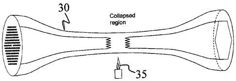
A fiber taper 30 was made using a fused biconic tapered coupler fabrication
jig with a oxy-
hydrogen flame 35 as shown schematically in Fig. 2. The LMA-15 fibers 20 were
elongated
in the flame by moving two translation stages in opposite directions and
sweeping the flame
along the fiber length. Pulling speeds varied from 0.03 to 0.1 mm/s. The taper
30 was viewed
with an optical microscope to determine if the holes were collapsed. With no
hole closure, no
transmission loss was observed during taper fabrication that was above the
resolution limit of
the detection system (¨ 0.05 dB). The taper waist length was ¨ 12 mm with
waist diameters
varying between 30 to 55 gm.
The transmission and reflection spectra of a grating written in the few-holed
ESM-12-01 fiber
10 are shown in Fig. 3. For a given pulse energy, the grating strength would
saturate after
11
CA 02579828 2007-02-23
Doc. No. 102-26 CA
Patent
=
approximately a 5-minute exposure. The grating strength could be increased by
incrementing
the IR pulse energy rather than increasing the exposure time. Beyond 1200
.1/pulse, damage
to the fiber surface or interior holes resulted. Using FBG simulation software
from Apollo
Photonics, assuming a fundamental resonance and a Gaussian apodized beam
profile of length
L = 6.4 mm (FWHM L = 2.1 mm), the ¨6 dB transmission dip corresponds to a An 4
x 10-4,
From the Bragg relation MilB = 2neffAg where the order M= 3, the effective
index of the fiber
n eff = 1.442 at the Bragg resonance AB = 1544.5 mm No An dependence on the IR
beam
polarization was observed.
In the case of the LMA-15 fiber, neither adjustment of the fiber rotation to
optimize the
orientation of the microstructure with respect to the incident IR beam nor
increasing pulse
energy could overcome scattering of the writing beam without damaging the
fiber. Several
tapers were then fabricated. For the first taper, a slow pull speed of 0.03
mm/s resulted in a
tapering of the fiber down to a 30 gm diameter taper waist with hole closure
occurring over
the entire 12 mm length of the taper waist. Optical microscope images of the
collapsed region
show that there was no scattering of the light by the cladding holes (see Fig
4 a).
With 1100 .1/pulse and 200 Hz, the incident beam was swept once across the
cross section of
the fiber taper producing the multimode transmission spectrum shown in Fig. 5
after a 1
minute exposure. The strongest resonance is ¨ -20 dB. The grating inscribed in
the tapered
PCF was observed under the optical microscope normal to and along the laser
beam optical
axis (Fig. 4 b and c respectively). From microscope observations, the length
over which the
holes collapsed was short (¨ 100 gm) likely producing a tapering transition
that was not
adiabatic.
Another taper was fabricated with an increased pull speed of 0.1 mm/s that
resulted in a 55
p.m diameter taper but without closure of the cladding holes. The oxygen
content in the flame
was then increased to produce a hotter flame, resulting in a 10 mm length of
collapsed holes.
Using the same exposure conditions, a grating was inscribed after a 1 minute
exposure in the
collapsed-hole region producing a multimode reflection response as shown in
Fig. 6. The
12
CA 02579828 2007-02-23
Doc. No. 102-26 CA
Patent
strongest resonance is ¨ -9 dB in transmission. Both of the grating structures
shown in Fig. 4
and 6 are highly multimode implying that strong mode coupling results from the
collapse of
the holes. A microscope image of the grating in the taper is shown in Fig. 6c.
Without collapsing of the holes, no transmission of the incident 800 nm
radiation through the
taper could be observed for diameters <40 m. This may be due to the
generation of a partial
bandgap caused by the reduced hole spacing which is resonant with the incident
radiation [9].
Another grating was written in a 48 gm diameter LMA-15 fiber taper such that
the holes were
not collapsed, but the bandgap was no longer incident with the 800 rim grating
writing
wavelength, allowing for a partial transmission through the taper. Assuming
that the ratio of
hole size and spacing remains constant for the taper, a 1-D simulation of the
Fresnel
reflections resulting from the 7 rows of holes shows that for a 48 pm taper,
there is no
reflection at 800 iun. With transmission loss before grating fabrication <
0.05 dB, it is likely
that the core mode was still guided. The fiber was exposed to 1000 .I/pulse
and 200 Hz for ¨
80 seconds, resulting in a quasi-single mode grating response (see Fig. 7).
Using the same
FBG modeling package and assumptions used for the grating in Fig. 3, the
corresponding An
for the grating in Fig. 7 is ¨3 x 10⁴ with an neff= 1.423 for AB = 1524.1 rim.
In Fig. 7 considerable shifting of the Bragg resonance to shorter wavelength
is observed. Near
field images of the mode field diameter (MFD) of a 55 tun taper were obtained
using an IR
sensitive camera and a tunable laser source. Using the mode field measurement
from a
standard SMF-28 fiber as a reference (MFD = 10.4 pm for SMF-28 at 1550 rim),
the MFD of
the LPN mode of the taper was 7.3 p.m, slightly narrower than that of SMF-28
fiber (see Fig.
8). By tapering the fiber from 230 to 55 m, the core was similarly reduced
from 15 to 3.6
pm, therefore there is significant increase in mode overlap with the
microstructured cladding
region. The reduced confinement of the fundamental mode in the core region
results in a
greater contribution of the hole structures to the effective index, hence the
shift of the Bragg
resonance to shorter wavelengths.
13
CA 02579828 2013-07-16
Doc. No. 102-26 CA
Patent
Ideally one would prefer not to collapse the holes as the light propagating in
the collapsed region
becomes multimode. In the exit shoulder of the taper, light that is not in the
fundamental mode
becomes lost as the hole closure, at least in our case here, is not adiabatic.
It would ultimately
result in signal loss.
If loss due to the nonadiabaticity of the taper is not an issue, for example,
for a particular sensor
application, then collapsing holes definitely makes the grating inscription
easier, i.e. like
inscription in a glass rod.
It is possible to taper some photonic crystal fibers such as a "grape fruit"
style PCF adiabatically
with hole closure. In this instance, the grating inscription is easier. If the
holes are not
collapsed, the hole spacing can be adjusted by tapering so that the band gap
is not resonant with
the incident wavelength for a specific orientation of the holes with respect
to the incident beam.
In an alternative embodiment of this invention, the holes or voids within the
photonic crystal
fiber can be filled at least in a predetermined region with a fluid such as a
refractive index
matching oil so as to allow IR light to propagate through the cladding into
the core. As was
described heretofore, IR light incident upon the PCF from the side, that would
otherwise be
suitable to write a grating the core of a standard single or multimode optical
fiber will scatter due
to refractive index difference between the air in the holes and the glass
surrounding the holes. If
the index difference is lessened or essentially nulled, the light external to
the fiber directed to the
side of the PCF focused on the core will reach the core with little or no
scattering. Conveniently,
by placing an end of the PCF in a beaker of index matching oil, due to surface
tension the oil
wicks into and permeates the openings of the PCF. As well, a vacuum could be
applied to the
other end of the PCF to create suction in order to draw in the fluid; see Fig.
4 in US Patent
7,062,140.
14