Note : Les descriptions sont présentées dans la langue officielle dans laquelle elles ont été soumises.
CA 02583047 2011-03-16
SEMICONDUCTORS AND ELECTRONIC DEVICES GENERATED
THEREFROM
CROSS REFERENCE TO RELATED APPLICATIONS
[0001] U.S. Patent No. 7,372,071, filed April 6, 2006, on
Functionalized Heteroacenes and Electronic Devices Generated Therefrom,
by Yuning Li et al.
[0002] U.S. Patent Application Publication No. 2007-0260069, filed
April 6, 2006, on Functionalized Heteroacenes, by Yuning Li et al.
[0003] U.S. Patent No. 7,550,760, filed April 6, 2006, on Polyacenes
and Electronic Devices Generated Therefrom, by Yuning Li et al.
[0004] U.S. Patent No. 7,557,370, filed April 6, 2006, on Heteroacene
Polymers and Electronic Devices Generated Therefrom, by Yuning Li et al.
[0005] U.S. Patent No. 7,586,120, filed April 6, 2006, on Ethynylene
Acene Polymers and Electronic Devices Generated Therefrom, by Yuning Li
et al.
[0006] U.S. Patent No. 7,795,373, filed April 6, 2006, on Ethynylene
Acene Polymers, by Yuning Li et at.
[0007] U.S. Patent No. 7,449,715, filed April 6, 2006, on
Poly[bis(ethynyl)heteroacenes] and Electronic Devices Generated
Therefrom, by Yuning Li et at.
-1-
CA 02583047 2011-03-16
[0008] U.S. Patent No. 7,615,607, filed April 6, 2006, on
Semiconductor Polymers, by Yiliang Wu et at.
[0009] U.S. Patent No. 7,517,477, filed April 6, 2006, on
Polydiazaacenes and Electronic Devices Generated Therefrom, by Yiliang
Wu et al.
[0010] U.S. Patent No. 7,517,476, filed April 6, 2006, on
Polydiazaacenes, by Yiliang Wu et al.
[0011] U.S. Patent Application Publication No. 2007-0235719, filed
April 6, 2006, on Poly(alkynylthiophene)s and Electronic Devices Generated
Therefrom, by Beng S. Ong et at.
[0012] U.S. Patent No. 7,705,111, filed April 6, 2006, on
Poly(alkynylthiophene)s, by Beng S. Ong et at.
[0013] U.S. Patent No. 7,619,055, filed April 6, 2006, on Linked
Arylamine Polymers and Electronic Devices Generated Therefrom, by
Yuning Li et at.
[0014] U.S. Patent No. 7,847,052, filed April 6, 2006, on Linked
Arylamine Polymers, by Yuning Li et at.
[0015] Illustrated in U.S. Patent Application Publication No. 2006-
0124921, filed December 14, 2004 relating to indolocarbazole moieties and
thin film transistor devices thereof.
[0016] Illustrated in U.S. Patent No. 7,402,681, filed June 27, 2005
relating to indolocarbazole moieties and thin film transistor devices thereof.
[0017] Illustrated in U.S. Patent 6,770,904 and copending application
U.S. Patent No. 7,250,625, Publication No. 20050017311, are electronic
devices, such as thin film transistors containing semiconductor layers of, for
example, polythiophenes.
-2-
CA 02583047 2011-03-16
[0018] In aspects of the present disclosure, there may be selected the
appropriate substituents, such as a suitable hydrocarbon, a heteroatom
containing group, hydrogen, halogen, CN, NO2, rings, number of repeating
polymer units, number of groups, and the like as illustrated in the copending
applications.
[0019] The appropriate components, processes thereof and uses
thereof illustrated in these copending applications and patent may be
selected for the present invention in embodiments thereof.
STATEMENT REGARDING FEDERALLY SPONSORED RESEARCH OR
DEVELOPMENT
[0020] The electronic devices and certain components thereof were
supported by a United States Government Cooperative Agreement No.
70NANBOH3033 awarded by the National Institute of Standards and
Technology (NIST). The United States Government has certain rights
relating to the devices and certain semiconductor components illustrated
hereinafter.
BACKGROUND
[0021] The present disclosure is generally directed to semiconductors
of the formulas as illustrated herein and generated, for example, from
monomers containing two tertiary amines for stability primarily, and two
thieno groups, processes of preparation and uses thereof. More specifically,
the present disclosure in embodiments is directed to novel polymers of the
formulas as illustrated herein and generated, for example, from monomers
containing two tertiary amines for stability primarily, and two thieno groups
at
each end point of the monomer which permits, for example, extended
polymer conjugation after polymerization, and which can be
-3-
CA 02583047 2007-03-29
selected as solution processable and substantially stable channel
semiconductors in
organic electronic devices, such as thin film transistors.
[0022] There are desired electronic devices, such as thin film transistors,
TFTs, fabricated with a semiconductor of the formulas as illustrated herein,
and
which semiconductors possess excellent solvent solubility, and which can be
solution
processable; and which devices possess mechanical durability and structural
flexibility, characteristics which are desirable for fabricating flexible TFTs
on plastic
substrates. Flexible TFTs enable the design of electronic devices with
structural
flexibility and mechanical durability characteristics. The use of plastic
substrates
together with the semiconductor of the formulas as illustrated herein and
generated,
for example, from monomers containing two tertiary amines for stability
primarily,
and, for example, two thieno groups, can transform the traditionally rigid
silicon TFT
into a mechanically more durable and structurally flexible TFT design. This
can be of
particular value to large area devices such as large-area image sensors,
electronic
paper and other display media. Also, the selection of p-type semiconductors of
the
formulas as illustrated herein and generated, for example, from monomers
containing
two tertiary amines at the center portion of the monomeric unit of the polymer
structure for stability primarily, and two thieno end or termination groups of
the
monomeric unit of the polymer structure for extended conjugation for
integrated
circuit logic elements for low end microelectronics, such as smart cards,
radio
frequency identification (RFID) tags, and memory/storage devices, may enhance
their mechanical durability, and thus their useful life span.
[0023] A number of semiconductor materials are not, it is believed, stable
when exposed to air as they become oxidatively doped by ambient oxygen
resulting
in increased conductivity. The result is large off-current and thus low
current on/off
ratio for the devices fabricated from these materials. Accordingly, with many
of these
materials, rigorous precautions are usually undertaken during materials
processing
and device fabrication to exclude environmental oxygen to avoid or minimize
oxidative doping. These precautionary measures increase the cost of
manufacturing
-4-
CA 02583047 2007-03-29
therefore offsetting the appeal of certain semiconductor TFTs as an economical
alternative to amorphous silicon technology, particularly for large area
devices.
These and other disadvantages are avoided or minimized in embodiments of the
present disclosure.
REFERENCES
[0024] Regioregular polyhexylthiophenes usually undergo rapid photo
oxidative degradation under ambient conditions, while the know
polytriarylamines
possess some stability when exposed to air, however, these amines are believed
to
possess low field effect mobilities, disadvantages avoided or minimized with
the
polymers of the formulas as illustrated herein.
[0025] Also, acenes, such as pentacene, and heteroacenes are known to
possess acceptable high filed effect mobility when used as channel
semiconductors
in TFTs. However, these materials can be rapidly oxidized by, for example,
atmospheric oxygen under light, and such compounds are not considered
processable at ambient conditions. Furthermore, when selected for TFTs, acenes
have poor thin film formation characteristics and are substantially insoluble,
thus they
are essentially nonsolution processable; accordingly, such compounds have been
processed by vacuum deposition methods that result in high production costs,
eliminated or minimized with the TFTs generated with the semiconductors
illustrated
herein.
[0026] A number of organic semiconductor materials has been described for
use in field effect TFTs, which materials include organic small molecules,
such as
pentacene, see for example D.J. Gundlach et al., "Pentacene organic thin film
transistors - molecular ordering and mobility", IEEE Electron Device Lett.,
Vol. 18, p.
87 (1997); oligomers such as sexithiophenes or their variants, see for example
reference F. Gamier et al., "Molecular engineering of organic semiconductors:
Design
of self-assembly properties in conjugated thiophene oligomers", J. Amer. Chem.
-5-
CA 02583047 2007-03-29
Soc., Vol. 115, p. 8716 (1993), and poly(3-alkylthiophene), see for example
reference
Z. Bao et al., "Soluble and processable regioregular poly(3-hexylthiophene)
for field-
effect thin film transistor application with high mobility", App!. Phys. Lett.
Vol. 69,
p4108 (1996). Although organic material based TFTs generally provide lower
performance characteristics than their conventional silicon counterparts, such
as
silicon crystal or polysilicon TFTs, they are nonetheless sufficiently useful
for
applications in areas where high mobility is not required. These include large
area
devices, such as image sensors, active matrix liquid crystal displays and low
end
microelectronics such as smart cards and RFID tags.
[0027] TFTs fabricated from p-type semiconductor polymers of the formulas
illustrated herein may be functionally and structurally more desirable than
conventional silicons in that they may offer mechanical durability, structural
flexibility,
and the potential of being able to be incorporated directly onto the active
media of the
devices, thus enhancing device compactness for transportability. Also, a
number of
known small molecule or oligomer-based TFT devices rely on difficult vacuum
deposition techniques for fabrication. Vacuum deposition is selected primarily
because the materials selected are either insoluble or their solution
processing by
spin coating, solution casting, or stamp printing do not generally provide
uniform thin
films.
[0028] Further, vacuum deposition may also involve the difficulty of achieving
consistent thin film quality for large area format. Polymer TFTs, such as
those
fabricated from regioregular components, of, for example, regioregular poly(3-
alkylthiophene-2,5-diyl) by solution processes, while offering some mobility,
suffer
from their propensity towards oxidative doping in air. For practical low cost
TFT
design, it is therefore of value to have a semiconductor material that is both
stable
and solution processable, and where its performance is not adversely affected
by
ambient oxygen, for example, TFTs generated with poly(3-alkylthiophene-2,5-
diyl)
are sensitive to air. The TFTs fabricated from these materials in ambient
conditions
-6-
CA 02583047 2011-03-16
generally exhibit large off-current, very low current on/off ratios, and their
performance characteristics degrade rapidly.
[0029] Illustrated in Huang, D.H., et al, Chem. Mater. 2004, 16, 1298-
1303, are, for example, LEDS and field effect transistors based on certain
phenothiaazines like poly(10-(2-ethylhexyl)phenothiaazine).
[0030] Illustrated in Zhu, Y., et al, Macromolecules 2005, 38, 7983-
7991, are, for example semiconductors based on phenoxazine conjugated
polymers like poly(10-hexylphenoxazine).
[0031] Additional references that may be of interest include U.S. Patent
Nos. 6,150,191; 6,107,117; 5,969,376; 5,619,357, and 5,777,070.
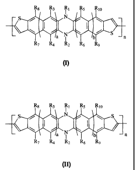
[0031 a] In accordance with another aspect, there is provided an
electronic device comprising a semiconductor selected from the group
consisting of at least one of Formula (I), Formula (II), or mixtures thereof
R8 R3 R1 R5 Rio
N
a N S
b n
R7 R4 R2 R6 9
(I)
Rg R3 Ri R5 Rio
N \ S
N b n
R7 R4 R2 R6 R9
(II)
-7-
CA 02583047 2011-03-16
wherein each R1 through R10 is independently hydrogen, alkyl, aryl, alkoxy,
halogen, arylalkyl, cyano, or nitro providing that R1 and R2 exclude halogen,
nitro and cyano; a and b represent the number of rings; and n represents the
number of repeating groups or moieties.
[0031 b] In accordance with a further aspect, there is provided a thin film
transistor comprised of a substrate, a gate electrode, a gate dielectric
layer, a
source electrode and a drain electrode, and in contact with the source/drain
electrodes and the gate dielectric layer a semiconductor layer comprised of at
least one semiconducting component having one of the following formulas
R8 R3 R1 R5 R10
N
-KD a N b S n
R7 R4 R2 R6 R9
m
R8 R3 Ri R5 R10
N S
N b n
R7 R4 R2 R6 R9
(In
wherein each R1 through R10 is independently hydrogen, alkyl, aryl, alkoxy,
halogen, arylalkyl, cyano, or nitro providing that R1 and R2 exclude halogen,
nitro and cyano; a and b represent the number of rings; and n represents the
number of repeating groups or moieties.
-7a-
CA 02583047 2011-03-16
[0031 c] In accordance with another aspect, there is provided an
electronic device comprising a semiconductive component and wherein said
device is a thin film transistor, and said component is selected from the
group
consisting of Formula (I), Formula (II) and mixtures thereof
R8 R3 Ri R5 Ric
N
a N b S n
R7 R4 R2 R6 R9
(1)
R8 R3 R1 R5 R10
N S
a N b n
R7 R4 R2 R6 9
(II)
wherein at least one of R1 to R10 is a suitable hydrocarbon; a and b represent
the number of rings; and n represents the number of repeating units.
BRIEF DESCRIPTION OF THE DRAWINGS
[0032] Illustrated in Figures 1 to 4 are various representative
embodiments of the present disclosure, and wherein p-type semiconductors
of the formulas as illustrated herein and generated, for example, from
monomers containing two tertiary amines for stability primarily, and two
thieno
groups for extended conjugation primarily are selected as the channel or
semiconductor material in thin film transistor (TFT) configurations.
-7b-
CA 02583047 2011-03-16
DESCRIPTION OF THE EXEMPLARY EMBODIMENTS
[0033] It is a feature of the present disclosure to provide p-type
semiconductors of the formulas as illustrated herein which are useful for
microelectronic device applications, such as TFT devices.
[0034] It is another feature of the present disclosure to provide p-type
semiconductors of the formulas as illustrated herein with a band gap of from
about 1.5 eV to about 3 eV as determined from the absorption spectra of thin
films thereof.
[0035] In yet a further feature of the present disclosure there is
provided p-type semiconductors of the Formulas I and II illustrated herein
which are useful as
-7c-
CA 02583047 2007-03-29
microelectronic components, and which polymers possess a solubility of, for
example, at least about 0.1 percent to about 95 percent by weight in common
organic
solvents, such as methylene chloride, tetrahydrofuran, toluene, xylene,
mesitylene,
chlorobenzene, dichlorobenzene, trichlorobenzene and the like, and thus these
polymers can be economically fabricated by solution processes such as spin
coating,
screen printing, stamp printing, dip coating, solution casting, jet printing,
and the like.
[0036] Another feature of the present disclosure resides in providing
electronic
devices, such as TFTs, with p-type semiconductors of the formulas as
illustrated
herein as channel layer, and which layer has a conductivity of from about 10-4
to
about 10-9 S/cm (Siemens/centimeter).
[0037] Also, in yet another feature of the present disclosure there are
provided
novel p-type semiconductors of the formulas as illustrated herein and devices
thereof, and which devices exhibit enhanced resistance to the adverse effects
of
oxygen, that is, these devices exhibit relatively high current on/off ratios,
and their
performance does not substantially degrade as rapidly as similar devices
fabricated
with regioregular poly(3-alkylthiophene-3,5-diyl) or with acenes.
[0038] Additionally, in a further feature of the present disclosure there is
provided a class of novel p-type semiconductors of the formulas as illustrated
herein
with unique structural features which are conducive to molecular self-
alignment under
appropriate processing conditions, and which structural features also enhance
the
stability of device performance. Proper molecular alignment can permit higher
molecular structural order in thin films, which can be important to efficient
charge
carrier transport, thus higher electrical performance.
[0039] There are disclosed in embodiments a polymer, and more specifically,
p-type semiconductors of the formulas as illustrated herein and electronic
devices
thereof. More specifically, the present disclosure relates to semiconductor
polymers
illustrated by or encompassed by Formula (I)
-8-
CA 02583047 2007-03-29
R8 R3 Ri R5 Rio
S N
\ I I /
a N b n
R7 R4 R2 R6 R9
(I)
or by Formula (II)
R8 R3 RI R5 Rio
S N S
a N b n
R7 R4 R2 R6 R9
(II)
wherein the monomeric unit of Formula (II) is an isomer of the monomeric unit
of
Formula (I), wherein, for example, each R1 through R10 is independently
hydrogen,
alkyl, aryl, alkoxy, arylalkyl, alkyl substituted aryls, except that R, and R2
exclude
halogen, cyano, nitro and the like; a and b represent the number of rings,
each of
them being, for example, from 0 to about 3; and n represents the number of
units,
such as for example, n is a number of from about 2 to about 2,000, and more
specifically, from about 2 to about 1,000, or from about 100 to about 700, or
from
about 2 to about 50, or mixtures of I and II, for example, from about 5
percent to
about 95 percent by weight of I and from about 95 to about 5 percent of II.
[0040] The number average molecular weight (Mn) of the polymer in
embodiments can be, for example, from about 500 to about 300,000, including
from
about 500 to about 100,000, and the weight average molecular weight (Mw,)
thereof
can be from about 600 to about 500,000, including from about 600 to about
200,000,
both as measured by gel permeation chromatography using polystyrene standards.
-9-
CA 02583047 2007-03-29
[0041] In embodiments, a specific class of p-type channel semiconductors are
represented by the following formulas
Rz
N S
n
Ri
(1)
R2
N
S R1
(2)
R3 R1 5
S / I \ N / I \
n
R4 R2 R6
(3)
R3 R1 R5
S / \ N S
n
R4 R2 R6
(4)
wherein each R1 through R6 is, for example, independently hydrogen, a suitable
hydrocarbon like alkyl, aryl, alkoxy, arylalkyl, alkyl substituted aryls, and
the like; and
mixtures thereof; and n represents the number of units, such as for example, n
is a
number of from about 2 to about 5,000, and more specifically, from about 2 to
about
-10-
CA 02583047 2007-03-29
1,000 or from about 2 to about 700. In embodiments, R1 through R6 are, more
specifically, alkyl, arylalkyl, and alkyl substituted aryls. Yet more
specifically, R1 and
R2 are alkyl with about 5 to about 20 carbon atoms of, for example, pentyl,
hexyl,
heptyl, octyl, nonyl, decyl, undecyl, dodecyl, tridecyl, tetradecyl,
pentadecyl,
hexadecyl, heptadecyl or octadecyl; arylalkyl with about 7 to about 26 carbon
atoms
of, for example, methylphenyl (tolyl), ethylphenyl, propyiphenyl, butylphenyl,
pentylphenyl, hexyiphenyl, heptylphenyl, octylphenyl, nonyiphenyl,
decylphenyl,
undecylphenyl, dodecylphenyl, tridecylphenyl, tetrad ecyl p henyl,
pentadecylphenyl,
hexadecyiphenyl, heptadecylphenyl, and octadecyiphenyl.
[0042] In embodiments there are disclosed processes for the preparation of p-
type semiconductors of the formulas as illustrated herein in accordance, for
example,
with the following reaction scheme
Scheme 1
3 RZ RS R3 RZ RS
N S N S
/ \ I \ / S A S \ ( \ A
N N
1 I
R4 Rl R6 R4 Rl R6
(III) (IV) A= Cl, Br, or I
FeC13
Dehaloge tive coupling
R3 RZ RS
/ N
S N
1 n
R4 Rl R6
(V)
-11-
CA 02583047 2007-03-29
[0043] More specifically, the process for the preparation of the polymer
semiconductor of the formulas as illustrated herein can be accomplished by,
for
example, the oxidative coupling polymerization of monomer (III) in the
presence of
oxidative coupling agent of, for example, FeCI3 at elevated temperatures of,
for
example, from room temperature to about 80 C, or by the dehalogenative
coupling
polymerization of monomer (IV) in the presence of zinc, nickel(II) chloride,
2,2'-
dipyridil, and triphenylphosphine in dimethylacetamide (DMAc) at elevated
temperatures of, for example, from about 70 C to about 90 C, and more
specifically,
about 80 C for a suitable period of time, like 24 hours. In Scheme 1, each R,
through
Rs is as illustrated herein like hydrogen, alkyl, aryl, alkoxy, arylalkyl,
alkyl substituted
aryls, and the like; and mixtures thereof; and n represents the number of
units, such
as for example, n is a number of from about 2 to about 500, and more
specifically,
from about 2 to about 1,000, or from about 2 to about 700.
[0044] Examples of each of the R groups (including R, through RIO) include
alkoxy and alkyl with, for example, from about 1 to about 30, including from
about 4
to about 18 carbon atoms (included throughout are numbers within the range,
for
example 4, 5, 6, 7, 8, 9, 10, 11, 12, 13, 14, 15, 16, 17 and 18), and further
including
from about 6 to about 16 carbon atoms, such as methyl, ethyl, propyl, butyl,
pentyl,
hexyl, heptyl, octyl, nonyl, decyl, undecyl, dodecyl, tridecyl, tetradecyl,
pentadecyl,
hexadecyl, heptadecyl, octadecyl, nonadecyl, or eicosanyl, isomeric forms
thereof,
mixtures thereof, and the like, and the corresponding alkoxides, such as
propoxy and
butoxy; alkylaryl with from about 7 to about 50 carbon atoms, from about 7 to
about
37 carbon atoms, from about 12 to about 25 carbon atoms, such as alkyl phenyls
like
methyl phenyl, substituted phenyls; aryl with from 6 to about 48 carbon atoms
and,
more specifically, with from about 6 to about 18 carbon atoms, such as phenyl.
Halogen includes chloride, bromide, fluoride and iodide. Heteroatoms and
hetero
containing groups include, for example, polyethers, trialkylsilyls,
heteroaryls, and the
like; and more specifically, thienyl, furyl and pyridiaryl. The hetero
component can be
-12-
CA 02583047 2007-03-29
selected from a number of known atoms like sulfur, oxygen, nitrogen, silicon,
selenium, and the like.
[0045] Specific illustrative polymer semiconductors are
C12H25
N
I l
S \ N \
n
C12H25
(5)
C12H25
N S
S N n
C12H25
(6)
C12H25
N
<-\ N \ QS
I n
C12H25
(7)
-13-
CA 02583047 2007-03-29
C8H17
S (8)
wherein n is, for example, from about 2 to about 50.
[0046] The polymer semiconductors are soluble or substantially soluble in
common coating solvents, for example, in embodiments they possess a solubility
of
at least about 0.1 percent by weight, and more specifically, from about 0.5
percent to
about 10 percent, or to about 95 percent by weight in such solvents as
methylene
chloride, 1,2-dichloroethane, tetrahydrofuran, toluene, xylene, mesitylene,
chlorobenzene, dichlorobenzene, and the like. Moreover, p-type semiconductors
of
the formulas as illustrated herein and generated, for example, from monomers
containing two tertiary amines for stability primarily, and two thieno groups
for
extended conjugation of the present disclosure in embodiments when fabricated
as
semiconductor channel layers in TFT devices provide a stable conductivity of,
for
example, from about 10-9 S/cm to about 104 S/cm, and more specifically, from
about
10-8 S/cm to about 10-5 S/cm as determined by conventional four-probe
conductivity
measurements.
[0047] It is believed that p-type semiconductors disclosed when fabricated
from solutions as thin films of, for example, from about 10 nanometers to
about 500
nanometers or from about 50 to about 300 nanometers in thickness materials are
more stable in ambient conditions than similar devices fabricated from poly(3-
al kylthiophene-2,5-diyl). When unprotected, the aforementioned p-type
semiconductors of the formulas as illustrated herein and devices thereof are
-14-
CA 02583047 2007-03-29
generally stable for a number of weeks rather than days or hours as is the
situation
with poly(3-alkylthiophene-2,5-diyl) after exposure to ambient oxygen, thus
the
devices fabricated from p-type semiconductors of the formulas as illustrated
herein
and generated, for example, from monomers containing two tertiary amines for
stability primarily, and two thieno groups in embodiments of the present
disclosure
can provide higher current on/off ratios, and their performance
characteristics do not
substantially change as rapidly as poly(3-alkylthiophene-2,5-diyl) when no
rigorous
procedural precautions have been taken to exclude ambient oxygen during
material
preparation, device fabrication, and evaluation. P-type semiconductors
disclosed are
in embodiments stable, that is they do not substantially degrade when exposed
to
oxygen.
[0048] Aspects of the present disclosure relate to an electronic device
comprising a semiconductor selected from the group consisting of at least one
of
Formula (I), Formula (II), or mixtures thereof
R8 R3 Rl R5 Rio
S N
a N b S n
7 R4 R2 R6 R9
(I)
R8 R3 Rl R5 Rio
S / N \ S
a N b ~fn
R7 R4 R2 R6 R9
(II)
wherein each R1 through R10 is independently hydrogen, alkyl, aryl, alkoxy,
halogen,
arylalkyl, cyano, or nitro providing that R, and R2 exclude halogen, nitro and
cyano; a
and b represent the number of rings; and n represents the number of repeating
-15-
CA 02583047 2007-03-29
groups or moieties; a thin film transistor comprised of a substrate, a gate
electrode, a
gate dielectric layer, a source electrode and a drain electrode, and in
contact with the
source/drain electrodes and the gate dielectric layer a semiconductor layer
comprised of at least one component or mixtures thereof of the following
formulas
R8 R3 RI R5 Rio
S N
a N b S n
R7 R4 R2 R6 R9
(I)
R8 R3 Rl R5 Rio
S N S
N b n
R7 R4 R2 R6 R9
(II)
wherein each R1 through R10 is independently hydrogen, alkyl, aryl, alkoxy,
halogen,
arylalkyl, cyano, or nitro providing that R, and R2 exclude halogen, nitro and
cyano; a
and b represent the number of rings; and n represents the number of repeating
groups or moieties; an electronic device comprising a semiconductive component
and wherein said device is a thin film transistor, and said component is
selected from
the group consisting of or mixtures thereof
R8 R3 R1 R5 Rio
S N
N b S n
R7 R4 R2 R6 R9
(I)
-16-
CA 02583047 2007-03-29
R8 R3 Ri R5 Rio
N S
a N b n
R7 R4 RZ R6 R9
(II)
wherein at least one of Ri to R10 is a suitable hydrocarbon; a and b represent
the
number of rings; and n represents the number of repeating units; a polymer
comprising those selected from the group consisting of at least one of Formula
(I),
Formula (II), or mixtures thereof
R8 R3 R1 R5 Rio
N
a N b S n
R7 R4 RZ R6 R9
(I)
R8 R3 Rl R5 R10
S N \ S
a N b
R7 R4 RZ R6 R9
(II)
wherein each R1 to R10 is independently hydrogen, alkyl, aryl, alkoxy,
halogen,
arylalkyl, cyano, or nitro providing that R, and R2 exclude halogen, nitro and
cyano; a
and b represent the number of rings; and n represents the number of repeating
groups or moieties; a TFT device wherein the substrate is a plastic sheet of a
polyester, a polycarbonate, or a polyimide; the gate source and drain
electrodes are
each independently comprised of gold, nickel, aluminum, platinum, indium
titanium
oxide, or a conductive polymer, and the gate dielectric is a dielectric layer
comprised
-17-
CA 02583047 2007-03-29
of silicon nitride or silicon oxide; a TFT device wherein the substrate is
glass or a
plastic sheet; said gate, source and drain electrodes are each comprised of
gold, and
the gate dielectric layer is comprised of the organic polymer
poly(methacrylate), or
poly(vinyl phenol); a device wherein the poly(3-alkynylthiophene) layer is
formed by
solution processes of spin coating, stamp printing, screen printing, or jet
printing; a
device wherein the gate, source and drain electrodes, the gate dielectric, and
semiconductor layers are formed by solution processes of spin coating,
solution
casting, stamp printing, screen printing, or jet printing; and a TFT device
wherein the
substrate is a plastic sheet of a polyester, a polycarbonate, or a polyimide,
and the
gate, source and drain electrodes are fabricated from the organic conductive
polymer
polystyrene sulfonate-doped poly(3,4-ethylene dioxythiophene), or from a
conductive
ink/paste compound of a colloidal dispersion of silver in a polymer binder,
and the
gate dielectric layer is organic polymer or inorganic oxide particle-polymer
composite;
device or devices include electronic devices such as TFTs.
DESCRIPTION OF THE FIGURES
[0049] In Figure 1 there is schematically illustrated a TFT configuration 10
comprised of a substrate 16, in contact therewith a metal contact 18 (gate
electrode),
and a layer of an insulating dielectric layer 14 with the gate electrode
having a portion
thereof or the entire gate in contact with the dielectric layer 14 on top of
which layer
14 two metal contacts, 20 and 22 (source and drain electrodes), are deposited.
Over
and situated between the metal contacts 20 and 22 is the p-type semiconductor
of
Formula (5) wherein n is 50, layer 12. The gate electrode can be included in
the
substrate, in the dielectric layer, and the like throughout.
[0050] Figure 2 schematically illustrates another TFT configuration 30
comprised of a substrate 36, a gate electrode 38, a source electrode 40, and a
drain
electrode 42, an insulating dielectric layer 34, and p-type semiconductor
layer 32 of
Formula (5) wherein n is 50.
-18-
CA 02583047 2007-03-29
[0051] Figure 3 schematically illustrates a further TFT configuration 50
comprised of a heavily n-doped silicon wafer 56, which can act as a gate
electrode, a
thermally grown silicon oxide dielectric layer 54, p-type semiconductor layer
52 of
Formula (5) wherein n is 50, on top of which are deposited a source electrode
60 and
a drain electrode 62; and a gate electrode contact 64.
[0052] Figure 4 schematically illustrates a TFT configuration 70 comprised of
substrate 76, a gate electrode 78, a source electrode 80, a drain electrode
82, p-type
semiconductors of the formulas as illustrated herein semiconductor layer 72 of
Formula (5) wherein n is 50, and an insulating dielectric layer 74.
[0053] Also, other devices not disclosed, especially TFT devices, are
envisioned, reference for example known TFT devices.
[0054] In some embodiments of the present disclosure, an optional protecting
layer may be incorporated on top of each of the transistor configurations of
Figures 1,
2, 3 and 4. For the TFT configuration of Figure 4, the insulating dielectric
layer 74
may also function as a protecting layer.
[0055] In embodiments and with further reference to the present disclosure
and the Figures, the substrate layer may generally be a silicon material
inclusive of
various appropriate forms of silicon, a glass plate, a plastic film or a
sheet, and the
like depending on the intended applications. For structurally flexible
devices, a
plastic substrate, such as for example polyester, polycarbonate, polyimide
sheets,
and the like, may be selected. The thickness of the substrate may be, for
example,
from about 10 micrometers to over 10 millimeters with a specific thickness
being from
about 50 to about 100 micrometers, especially for a flexible plastic
substrate, and
from about 1 to about 10 millimeters for a rigid substrate such as glass or
silicon.
[0056] The insulating dielectric layer, which can separate the gate electrode
from the source and drain electrodes, and in contact with the semiconductor
layer,
can generally be an inorganic material film, an organic polymer film, or an
organio-
inorganic composite film. The thickness of the dielectric layer is, for
example, from
about 10 nanometers to about 1 micrometer with a more specific thickness being
-19-
CA 02583047 2007-03-29
about 100 nanometers to about 500 nanometers. Illustrative examples of
inorganic
materials suitable as the dielectric layer include silicon oxide, silicon
nitride,
aluminum oxide, barium titanate, barium zirconate titanate, and the like;
illustrative
examples of organic polymers for the dielectric layer include polyesters,
polycarbonates, poly(vinyl phenol), polyimides, polystyrene,
poly(methacrylate)s,
poly(acrylate)s, epoxy resin, and the like; and illustrative examples of
inorganic-
organic composite materials include nanosized metal oxide particles dispersed
in
polymers, such as polyester, polyimide, epoxy resin and the like. The
insulating
dielectric layer is generally of a thickness of from about 50 nanometers to
about 500
nanometers depending on the dielectric constant of the dielectric material
used.
More specifically, the dielectric material has a dielectric constant of, for
example, at
least about 3, thus a suitable dielectric thickness of about 300 nanometers
can
provide a desirable capacitance, for example, of about 10-9 to about 10-7
F/cm2.
[0057] Situated, for example, between and in contact with the dielectric layer
and the source/drain electrodes is the active semiconductor layer comprised of
p-
type semiconductors of the formulas as illustrated herein, and wherein the
thickness
of this layer is generally, for example, about 10 nanometers to about 1
micrometer, or
about 40 to about 100 nanometers. This layer can generally be fabricated by
solution
processes such as spin coating, casting, screen, stamp, or jet printing of a
solution of
p-type semiconductors of the present disclosure.
[0058] The gate electrode can be a thin metal film, a conducting polymer film,
a conducting film generated from a conducting ink or paste, or the substrate
itself (for
example heavily doped silicon). Examples of gate electrode materials include,
but
are not limited to aluminum, gold, chromium, indium tin oxide, conducting
polymers,
such as polystyrene sulfonate-doped poly(3,4-ethylenedioxythiophene)
(PSS/PEDOT), a conducting ink/paste comprised of carbon black/graphite or
colloidal
silver dispersion contained in a polymer binder, such as Electrodag available
from
Acheson Colloids Company, and silver filled electrically conductive
thermoplastic ink
available from Noelle Industries, and the like. The gate layer can be prepared
by
-20-
CA 02583047 2007-03-29
vacuum evaporation, sputtering of metals or conductive metal oxides, coating
from
conducting polymer solutions or conducting inks or dispersions by spin
coating,
casting or printing. The thickness of the gate electrode layer is, for
example, from
about 10 nanometers to about 10 micrometers, and a specific thickness is, for
example, from about 10 to about 200 nanometers for metal films and about 1 to
about 10 micrometers for polymer conductors.
[0059] The source and drain electrode layer can be fabricated from materials
which provide a low resistance ohmic contact to the semiconductor layer.
Typical
materials suitable for use as source and drain electrodes include those of the
gate
electrode materials such as gold, nickel, aluminum, platinum, conducting
polymers,
and conducting inks. Typical thickness of this layer is, for example, from
about 40
nanometers to about 1 micrometer with the more specific thickness being about
100
to about 400 nanometers. The TFT devices contain a semiconductor channel with
a
width W and length L. The semiconductor channel width may be, for example,
from
about 10 micrometers to about 5 millimeters with a specific channel width
being
about 100 micrometers to about 1 millimeter. The semiconductor channel length
may
be, for example, from about 1 micrometer to about 1 millimeter with a more
specific
channel length being from about 5 micrometers to about 100 micrometers.
[0060] The source electrode is grounded and a bias voltage of generally, for
example, about 0 volt to about -80 volts is applied to the drain electrode to
collect the
charge carriers transported across the semiconductor channel when a voltage of
generally, for example, about +10 volts to about -80 volts is applied to the
gate
electrode.
[0061] Other known materials not recited herein for the various components of
the TFT devices of the present disclosure can also be selected in embodiments.
[0062] Although not desiring to be limited by theory, it is believed that the
tertiary amine center groups function primarily to minimize or avoid
instability
because of exposure to oxygen and thus increase the oxidative stability of the
semiconductor of the formulas as illustrated herein and generated, for
example, from
-21-
CA 02583047 2007-03-29
monomers containing two tertiary amines for stability primarily, and two
thieno end
groups in solution under ambient conditions and the substituents, such as
alkyl,
permit the solubility of these polymers in common solvents, such as ethylene
chloride.
[0063] The claims, as originally presented and as they may be amended,
encompass variations, alternatives, modifications, improvements, equivalents,
and
substantial equivalents of the embodiments and teachings disclosed herein,
including
those that are presently unforeseen or unappreciated, and that, for example,
may
arise from applicants/patentees and others. Unless specifically recited in a
claim,
steps or components of claims should not be implied or imported from the
specification or any other claims as to any particular order, number,
position, size,
shape, angle, color, or material.
-22-