Note : Les descriptions sont présentées dans la langue officielle dans laquelle elles ont été soumises.
CA 02614604 2008-01-08
WO 2007/072226 PCT/IB2006/004050
,CMOS Full Wave Rectifier
[0001] Field of the Invention
[0002] The present invention relates to a rectifier circuit, and more
particularly, to a
CMOS full-wave rectifier circuit.
Background Art
[0003] Generally, rectifiers are used for the conversion of AC to DC voltage.
A
conventional full-wave rectifier that includes a diode bridge 105 is shown in
Fig. 1. The
diode bridge 105 can be regarded as a non-linear, two-port device having an
input voltage
ul(t), an output voltage u2(t), and four diodes 101, 102, 103, and 104. In
general, the
output port is connected to a load 106. If the load 106 is a purely resistive
load 107, then
the sign of the input voltage ul(t) defines the current path through the
rectifier 105, i.e.,
whether the current is flowing through diodes 101 and 102, or through diodes
103 and
104. However, the current through load 107 has the same direction in both
cases. The
resulting voltage u2(t) is given by:
u2 (t) = lul (t)I - 2uD , if lu, (t)I > 2UD, and (1 a)
u2(t) = 0, if lul (t)I < 2uD, (lb)
where uD denotes the voltage drop across one diode. As a general disadvantage,
the
voltage drop across load 107 is not the full magnitude of the input voltage
difference
tul(t)j, but diminished by 2uD, i.e., by two diode voltage drops (typically,
1.4V). For low
power applications, the diode voltages may significantly contribute to the
overall power
consumption of the circuit.
[0004] The diode bridge shown in Fig. 1 is often used for supply voltage
generation. In
this case the load could be a resistor 108 (representing the power consumption
of a
complex electronic circuit) and a smoothing capacitor 109 connected in
parallel. For a
given frequency of the input signal ul(t), capacitor 109 usually is chosen
sufficiently large
to ensure a nearly constant supply voltage u2(t).
-1-
CA 02614604 2008-01-08
WO 2007/072226 PCT/IB2006/004050
Summary of the Invention
[0005] A rectifier and method for rectification includes a bridge that is
advantageously
implemented using switches as opposed to diodes. The switches may be, without
limitation, MOS transistors. Such a rectifier may be used, for example, in a
wide variety
of applications, such as medical or automotive applications.
[0006] In accordance with an embodiment of the invention there is provided a
rectifier
circuit which includes first and second input terminals for receiving a
rectangular wave
input voltage, and first and second output terminals for providing a rectified
dc output
voltage. A first switch is coupled between the first input terminal and a
first node, the first
node being coupled to the first output terminal. A second switch is coupled
between the
second input terminal and the first node. A third switch is coupled between
the first input
terminal and a second node, the second node being coupled to the second output
terminal.
A fourth switch is coupled between the second input terminal and to the second
node. The
first switch and fourth switch are gated on when the input voltage is of a
first polarity; and
the second switch and the third switch are gated on when the input voltage is
of a second
polarity opposite the first polarity so as to provide an output voltage having
a magnitude
substantially equal to the magnitude of the input voltage.
[0007] In accordance with related embodiments of the invention, the first
switch, the
second switch, the third switch, and the fourth switch may be MOS transistors.
For
example, the first switch and the second switch may be PMOS transistors, and
the third
switch and fourth switch may be NMOS transistors. The first switch and the
fourth switch
may be gated by one of the first input terminal and the second input terminal,
and the
second switch and the third switch may be gated by the other of the one of the
first input
terminal and the second input terminal. A parallel load combination of a
resistance and a
capacitance may be coupled to the rectifier circuit between the first and
second output
terminals. Or a resistive load may be coupled to the rectifier circuit between
the first and
second output terminals without a discrete parallel capacitor. Both the load
and the
rectifier circuit may be integrated on a single chip. The circuit may be used
to ensure a
desired supply voltage polarity.
-2-
CA 02614604 2008-01-08
WO 2007/072226 PCT/IB2006/004050
[0008] In accordance with another embodiment of the invention, a polarity
protection
circuit includes the rectifier circuit of the above-described embodiments. In
another
embodiment, an implanted medical device, such as a retinal implant or a
cochlear implant,
includes the rectifier circuit of the above-described embodiments. In
accordance with still
another embodiment of the invention, a chip includes both the rectifier
circuit of the
above-described embodiments and a parallel load combination of a resistance
and a
capacitance coupled between the first and second output terminals. Or the load
may be a
resistive load without a discrete parallel capacitor. The load may include a
signal
processor.
[0009] In accordance with yet another embodiment of the invention, a method of
rectifying is presented. The method includes applying a rectangular input
signal between
a first input terminal and a second input terminal. A first switch is coupled
between the
first input terminal and a first node, and a second switch is coupled between
the second
input terminal and the first node. The first node is coupled to a first output
terminal. A
third switch is coupled between the first input terminal and a second node,
and a fourth
switch is coupled between the second input terminal and the second node. The
second
node is coupled to a second output terminal. The first switch and fourth
switch are gated
on when the input signal is of a first polarity; while the second switch and
the third switch
are gated on when the input signal is of a second polarity opposite the first
polarity so that
the first and second output terminals provide a rectified dc voltage having a
magnitude
substantially equal to the magnitude of the input voltage.
[0010] In accordance with related embodiments of the invention, the first
switch, the
second switch, the third switch, and the fourth switch may be MOS transistors.
The first
switch and the second switch may be PMOS transistors, and the third switch and
fourth
switch may be NMOS transistors. The first switch and the fourth switch may be
gated by
one of the first input terminal and the second input terminal, and the second
switch and the
third switch may be gated by the other of the one of the first input terminal
and the second
input terminal. The method may further comprise coupling a parallel load
combination of
a resistance and a capacitance between the first and second output terminals.
Or the
-3-
CA 02614604 2008-01-08
WO 2007/072226 PCT/IB2006/004050
method may further comprise coupling a resistive load between the first and
second output
terminals without a discrete parallel capacitor. In a further embodiment, the
input signal
may be disconnected from the input terminals for a period of time after the
switches are
gated on.
Brief Description of the Drawings
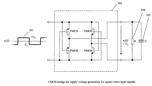
[0011] Fig. 1 is a schematic showing a full-wave bridge rectifier with varying
loads (Prior
Art);
[0012] Fig. 2 is a schematic showing a CMOS-bridge with varying loads, in
accordance
with an embodiment of the invention; and
[0013] Fig. 3 is a schematic showing a CMOS-bridge for supply voltage
generation for
square wave input signals, in accordance with an embodiment of the invention.
[0014] Fig. 4 shows a rectangular wave input signal having active and floating
periods
according to one embodiment of the invention.
Detailed Description of Specific Embodiments
[0015] In illustrative embodiments, a rectifier includes a bridge that is
implemented using
switches. The switches may be, for exarnple, MOS transistors. Details of
illustrative
embodiments are discussed below.
[0016] Fig. 2 is a schematic showing a CMOS-bridge with varying loads, in
accordance
with an exemplary embodiment of the invention. The arrangement of transistors
as shown
in Fig. 2 represents a non-linear two-port device 205 with input voltage ul(t)
and output
voltage u2(t). As compared to the diode bridge of'Fig. 1, the four diodes are
replaced by
four transistors, i.e., by two PMOS-transistors 201 and 203, and two NMOS
transistors
202 and 204, which are operated as ON/OFF-switches. It is to be understood
that in
various embodiments the MOS transistors may be replaced by other types of
switching
technologies which may be, for example, electrical, mechanical, biological or
molecular in
nature, and that the present invention is not limited to MOS technology.
-4-
CA 02614604 2008-01-08
WO 2007/072226 PCT/IB2006/004050
[0017] As shown in Fig. 2 the output terminals 211 and 212 of the two-port
device 205
may be connected to a load 206. The load 206 may be, for example, a resistive
load 207,
or a resistive load 208 in parallel with a capacitive load 209. Both the two-
port device 205
and the load 206 may be advantageously integrated on single chip. For example,
the two-
port device 205 may be electrically coupled with other circuitry, such as a
signal
processor, the two-port device 205 and signal processing circuitry integrated
on a single
chip.
[0018] The gates of the transistors may be directly connected to the input
voltage rails.
Assuming a purely resistive load 207, and an ideal switching performance of
the
transistors, the following conditions are fulfilled:
U2 (t) = U1(t)I , if IU1(t)I > uTliR , a.nd (2a)
uz (t) = 0, if Jul (t)I < u.iMR , (2b)
whereby voltage UTHR denotes a MOS-threshold voltage, which here is assumed to
be
equal for both, PMOS and NMOS transistors. For u, (t) - uTmR , transistors 201
and 202
are switched on (low impedance), whereas transistor 203 and 204 are switched
off (high
impedance), and vice versa for u, (t) 5-uTmR, transistors 203 and 204 are
switched on,
and transistors 201 and 202 are switched of~ Thus, for the special case of an
ohmic load,
the CMOS-bridge of Fig. 2 represents a full-wave rectifier, similar to the
diode bridge Fig.
1. Note that here the full input voltage magnitude applies at load 207, and
there is no
reduction due to diode voltage drops. Typically, MOS threshold voltages are
uTxR - 0.7V.
[0019] For the implementation of bridge Fig. 2, standard CMOS-technology can
be used.
For example, using N-well technology, the P-silicon substrate material is
connected to the
negative potential 211, and the N-wells are connected to the positive
potential 212 of the
output port. In various embodiments, the four transistors may be sufficiently
large to
ensure a small voltage drop during the switch ON-states. If these voltage
drops are too
large (typically, larger than about 0.7V), then para"sitic substrate PN-diodes
get conductive,
adversely affecting operation of a chip, for example, that includes both the
two port 205
and load 206.
-5-
CA 02614604 2008-01-08
WO 2007/072226 PCT/IB2006/004050
[0020] Assuming a sinusoidal input voltage, the CMOS-bridge 205 in Fig. 2 does
not fully
work as a rectifier for all types of loads. The reason is that transistors
operated in
ON-states allow current flowing in both directions - in contrast to a diode.
For example, if
the load 206 is composed of a resistor 208 and a smoothing capacitor 209 in
parallel, then
the capacitor is partly discharged via transistors in switch-turn-ON states.
Assuming
U1(t) > UTHR, transistors 201 and 202 are switched on, and in this situation,
voltage u2(t)
simply follows the input voltage ul(t). This means that the capacitor 209 is
discharged not
only via the resistor 208, but also via the input lines. However, a true
rectifier
characteristic is obtained again, if a diode 210 is connected in series to
resistor 208 and
capacitor 209. The advantage as compared to a diode-bridge Fig. 1 is that only
one diode
voltage drop appears instead of two.
[0021] Fig. 3 is a schematic showing a CMOS-bridge 302 for use, without
limitation, with
square- or rectangular-wave input signals, in accordance with an embodiment of
the
invention. As shown in Fig. 3, if the input voltage is not a sinusoidal, but a
square- or
rectangular-wave 301 with two levels U, , then CMOS-bridge 302 can be
operated as a
full-wave rectifier without an additional diode, even if the load is composed
of a resistor
304 and a capacitor 303. In this case the output voltage is u2(t) - Ul.
Resistor 304 may
represent the power consumption of a complex electronic circuit.
[0022] While Fig. 3 shows a square wave signal being applied to an embodiment,
the input
may usefully be a more general rectangular wave signal. In the general case of
a
rectangular wave input signal, embodiments would not necessarily require a
discrete
capacitive component such as output capacitor 303, such that the only output
capacitance
might be relatively small parasitic capacitances from components and leads.
[0023] Moreover, for the circuit shown in Fig. 3, when the input terminals
have a high
impedance across them, as in the case where they are unconnected, the bridge
circuit may
possesses the interesting property of remaining stable in its existing logic
state. For
example, as shown in Fig. 4, assume that a +5 vdc input is applied to the
input terminals
-6-
CA 02614604 2008-01-08
WO 2007/072226 PCT/IB2006/004050
during the time period on the left labeled as "active." Then, the same +5 vdc
will be
passed to the output terminals and across output resistor 304 and output
capacitor 303.
Assuming that the input signal is then disconnected from the input terminals,
the PMOS
switch in the upper left and the NMOS switch in the lower right of the circuit
will remain
in a low impedance state, and, assuming the RC time constant of resistor 304
and capacitor
303 are sufficiently large, the put voltage will continue to float at +5 vdc
due to capacitor
303. The same thing happens oppositely on the right side of Fig. 4 during the
second
active and floating periods. This may be a useful property in some situations
such as low
power applications when it may be possible to apply the input signal for
relatively short
active periods and let the circuit float during succeeding inactive periods.
Such a signal
having active and floating periods need not necessarily be periodic, but in
some
applications may be non-periodic signal such as a data signal.
[0024] The CMOS-bridge in the above-described embodiments may advantageously
be
used in a wide variety of applications. For example, the CMOS-bridge may be
used to
provide rectification and/or to ensure a desired supply voltage polarity, in
diverse fields
such as, without limitation, the automotive or medical fields. For example, a
chip
containing such a CMOS bridge may be part of an implantable medical device
such as a
retinal implant system or a cochlear implant system. Embodiments may also
include using
such a circuit as the basis for a polarity protection circuit which allows for
arbitrary
connecting of the inputs to a dc source, independently of the polarity.
[0025] Although various exemplary embodiments of the invention have been
disclosed, it
should be apparent to those skilled in the art that various changes and
modifications can be
made which will achieve some of the advantages of the invention without
departing from
the true scope of the invention.
-7-