Note : Les descriptions sont présentées dans la langue officielle dans laquelle elles ont été soumises.
CA 02675081 2009-08-11
ELECTRONIC DEVICE COMPRISING SEMICONDUCTING POLYMERS
BACKGROUND
[0001] The present disclosure relates, in various embodiments, to
compositions and
processes suitable for use in electronic devices, such as thin film
transistors ("TFT"s).
The present disclosure also relates to components or layers produced using
such
compositions and processes, as well as electronic devices containing such
materials.
[0002] Thin film transistors (TFTs) are fundamental components in modern-
age
electronics, including, for example, sensors, image scanners, and electronic
display
devices. TFT circuits using current mainstream silicon technology may be too
costly for
some applications, particularly for large-area electronic devices such as
backplane
switching circuits for displays (e.g., active matrix liquid crystal monitors
or televisions)
where high switching speeds are not essential. The high costs of silicon-based
TFT
circuits are primarily due to the use of capital-intensive silicon
manufacturing facilities as
well as complex high-temperature, high-vacuum photolithographic fabrication
processes
under strictly controlled environments. It is generally desired to make TFTs
which have
not only much lower manufacturing costs, but also appealing mechanical
properties
such as being physically compact, lightweight, and flexible. Organic thin film
transistors
(OTFTs) may be suited for those applications not needing high switching speeds
or high
densities.
[0003] TFTs are generally composed of a supporting substrate, three
electrically
conductive electrodes (gate, source and drain electrodes), a channel
semiconducting
layer, and an electrically insulating gate dielectric layer separating the
gate electrode
from the semiconducting layer.
[0004] It is desirable to improve the performance of known TFTs.
Performance can
be measured by at least three properties: the mobility, current on/off ratio,
and threshold
voltage. The mobility is measured in units of cm2/V=sec; higher mobility is
desired. A
higher current on/off ratio is desired. Threshold voltage relates to the bias
voltage
needed to be applied to the gate electrode in order to allow current to flow.
Generally, a
threshold voltage as close to zero (0) as possible is desired.
1
-
CA 02675081 2009-08-11
=
[0005]
While p-type semiconducting materials have been extensively researched,
less emphasis has been applied to n-type semiconducting materials. N-type
organic
semiconductors having high electron mobility and stability in air, especially
solution
processable n-type semiconductors, are rare due to their air sensitivity and
difficulties in
synthesis compared to p-type semiconductors. Because n-type semiconductors
transport electrons instead of holes, they require a low Lowest Unoccupied
Molecular
Orbital (LUMO) energy level. To achieve low LUMO levels, electron-withdrawing
groups such as fluoroalkyl, cyano, acyl, or imide groups have been applied to
some n-
type organic semiconductors. However these electron-withdrawing groups can
only be
used as substituents or sidechains on conjugated cores such as acenes,
phthalocyanines, and oligothiophenes, and cannot be used as conjugated
divalent
linkages themselves for constructing linear n-type semiconducting polymers.
Most
reported high-mobility air-stable n-type semiconductors are small molecular
compounds
and can only be processed using expensive vacuum deposition techniques to
achieve
maximum performance.
BRIEF DESCRIPTION
[0006] The present disclosure is directed, in various embodiments, to
semiconducting polymers and to electronic devices, such as thin film
transistors, having
a semiconducting layer comprising the semiconducting polymer. The
semiconducting
polymers are n-type or both n-type and p-type semiconducting materials that
are stable
in air and have high mobility.
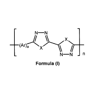
[0007] In embodiments is disclosed an electronic device comprising a
semiconducting layer, the semiconducting layer comprising a semiconducting
polymer
of Formula (I):
N¨N
¨(Ar)r(X
3(X
)
N¨N n
Formula (I)
2
CA 02675081 2009-08-11
wherein X is independently selected from S, Se, 0, and NR, wherein R is
independently
selected from hydrogen, alkyl, substituted alkyl, aryl, substituted aryl,
heteroaryl, and -
CN; Ar is independently a conjugated divalent moiety; a is an integer of from
1 to about
10; and n is an integer from 2 to about 5,000.
[0008] Each Ar is a conjugated divalent moiety selected from
Se
S R,
R'
R'
1000
(õ/)
I
R'
411F
Ole /
R' R'
R' R' R'
R' R' RI'
wherein R' is independently selected from hydrogen, alkyl, substituted alkyl,
aryl,
substituted aryl, heteroaryl, -CN, and the like, or mixtures thereof. In
specific
embodiments, R' is alkyl. The conjugated divalent moiety Ar may be substituted
once,
twice, or multiple times where applicable, with alkyl, substituted alkyl,
aryl, substituted
aryl, heteroaryl, halogen, -CN, -NO2, and the like, or mixtures thereof.
[0009] The semiconducting polymer may have a LUMO of 3.5 eV or less, or 4.0 eV
or less, or 4.5 eV or less, against vacuum.
[0010] In some embodiments, Ar may be
3
CA 02675081 2014-09-05
Ri
Ri
wherein R1 is an alkyl group having 1 to about 18 carbon atoms, or an aryl or
a
heteroaryl group having from about 5 to about 20 carbon atoms.
[0011] In other embodiments is disclosed a semiconducting polymer of
Formula (1):
N¨N
(Ar)-(X"----AV X)
Formula (I)
wherein X is independently selected from S, Se, 0, and NR, wherein R is
independently
selected from hydrogen, alkyl, substituted alkyl, aryl, substituted aryl,
heteroaryl, and -
CN; each Ar is independently selected from:
R' RA 5s R' R'
roaN
R'
S
R'
R' =
a is an integer from 1 to about 10; and n is an integer from 2 to about 5,000.
[0011a] In accordance with another aspect, there is provided a thin film
transistor
comprising a gate electrode, a source electrode, a drain electrode, a
dielectric layer, a
semiconducting layer, and an interfacial layer, wherein the dielectric layer
separates the
gate electrode from the semiconducting layer and the interfacial layer is
located between
the dielectric layer and the semiconducting layer, and wherein the
semiconducting layer
comprises a semiconducting polymer of Formula (1):
4
CA 02675081 2014-09-05
N¨N
/ 3(X)
[(Ar) x
\ / _
N¨N - n
Formula (I)
wherein X is independently selected from S, Se, 0, and NR, wherein R is
independently
selected from hydrogen, alkyl, substituted alkyl, aryl, substituted aryl,
heteroaryl, and -
CN;
a is an integer from Ito about 10;
n is an integer from 2 to about 5,000; and
each Ar is a conjugated divalent moiety selected from:
Ri\
Se N
RI
.7' ...7, loop _ 4000000
c1-->
N---i'N=
a
\ ilk /
R' R'
N
1
s S N
1
and combinations thereof, wherein R' is independently selected from hydrogen,
alkyl,
substituted alkyl, aryl, substituted aryl, heteroaryl, and -CN; and the
divalent moiety may
4a
CA 02675081 2014-09-05
be substituted peripherally with alkyl, substituted alkyl, aryl, substituted
aryl, heteroaryl,
halogen, -CN, or -NO2.
[0011b] In accordance with another aspect, there is provided a thin film
transistor
comprising a gate electrode a source electrode, a drain electrode, a
dielectric layer, a
semiconducting layer, and an interfacial layer, wherein the dielectric layer
separates the
gate electrode from the semiconducting layer and the interfacial layer is
located between
the dielectric layer and the semiconducting layer, and wherein the
semiconducting layer
comprises a semiconducting polymer of Formula (1):
N¨N
,94
N¨N n
Ri
Formula (1)
wherein R1 is an alkyl group having 1 to about 20 carbon atoms, or an aryl or
a
heteroaryl group having from about 5 to about 20 carbon atoms, and n is an
integer from
2 to about 5,000.
[0011c] In accordance with another aspect, there is provided a thin film
transistor
comprising a gate electrode a source electrode, a drain electrode, a
dielectric layer, a
semiconducting layer, and an interfacial layer, wherein the dielectric layer
separates the
gate electrode from the semiconducting layer and the interfacial layer is
located between
the dielectric layer and the semiconducting layer, and wherein the
semiconducting layer
comprises a semiconducting polymer, wherein the semiconducting polymer is
selected
from the group consisting of formulas (1), (3), (4), (6) through (9), (11)
through (17), (19)
through (25), and (27) through (32):
R1
¨194
\
N¨N
(1)
/ S
N¨N
R1 S /n
(3)
4b
(Li-)
N-N
uI S
s
N-N
S /
(6)
u, N-N
,(s))
s s ____
N-N
ej
(9)
1H
0/
/ s
N-N
vul
N-N .?A
1.H
(L)
u1 NN
0
NN
(9)
41
uNN
N-N
(v)
11,1
m.._N S
"
0,L0
u(/
)=1"-N1
SO-60-VTOZ T8OSL9Z0 VD
CA 02675081 2014-09-05
N-N
SI
\S---TrLS n
S NrN
R1
(12)
R2
N¨N
= = /6)
n
R2 R1 N¨N
(13)
Ni s
S \ (CS¨\\
N¨N n
R1
(14)
R'
N¨N
ONJO
N¨N ' n
N
(15)
R'
N¨N
0 11
N¨N
S
/ N
(16)
R1
S II
N¨N n
(17)
4d
CA 02675081 2014-09-05
s R1 R
\ NJ-1k
R1 S \
N¨N
(19)
R1
R\ N_N2
S N N n
I R
S N¨N
R1
(20)
R2 R1
N¨N \
n
I N¨N
R2 R1
(21)
R1
N N R
USA
-\\
N I NN n
R1
(22)
R'
N¨N
N /
0
N¨\\
I N¨N n
0
14'
(23)
R1
R'
N¨N
/ s n
N¨N A
s
N
4e
CA 02675081 2014-09-05
(24)
R1
N-N
S \ \\ g
N-N
R1
(25)
s
N-N
\ \ Se Ii
R1 S \ 'Se in
N-N
(27)
S Sei/L-Se)n
S N-11
R1
=
(28)
R2 R1
N-N
's)
R2
N-N n
R2 Ri
(29)
R1
õ N N-N
N-N n
R1
(30)
R' N-N
/
0
/ S6 \\ //
N-N in
0
F2'
(31)
4f
CA 02675081 2014-09-05
Ri
R'
0
N-N
Sy/
0
R'
R1
(32)
wherein R, R', R1, and R2 are independently selected from hydrogen, alkyl,
substituted
alkyl, aryl, substituted aryl, heteroaryl, -CN, or mixtures thereof, and n is
an integer from
2 to about 5,000.
[0011d] In accordance with another aspect, there is provided a thin film
transistor
comprising a gate electrode a source electrode, a drain electrode, a
dielectric layer, a
semiconducting layer, and an interfacial layer, wherein the dielectric layer
separates the
gate electrode from the semiconducting layer and the interfacial layer is
located between
the dielectric layer and-the semiconducting layer, and wherein the
semiconducting layer
comprises a semiconducting polymer of Formula (I):
N¨N
(Ar)r(X
Formula (I)
wherein X is independently selected from S, Se, 0, and NR, wherein R is
independently
selected from hydrogen, alkyl, substituted alkyl, aryl, substituted aryl,
heteroaryl, and -
ON;
each Ar is independently selected from:
R' R4
s
.õ =
4g
CA 02675081 2014-09-05
wherein R' is independently selected from hydrogen, alkyl, substituted alkyl,
aryl,
substituted aryl, heteroaryl, and -CN;
a is an integer from Ito about 10; and
n is an integer from 2 to about 5,000.
[0012] Also included in further embodiments are the semiconducting layers
and/or
thin film transistors produced by this process.
4h
CA 02675081 2009-08-11
[0013] These and other non-limiting characteristics of the exemplary
embodiments of
the present disclosure are more particularly described below.
BRIEF DESCRIPTION OF THE DRAWINGS
[0014] The following is a brief description of the drawings, which are
presented for
the purpose of illustrating the exemplary embodiments disclosed herein and not
for the
purpose of limiting the same.
[0015] FIG. 1 is a first exemplary embodiment of a TFT of the present
disclosure.
[0016] FIG. 2 is a second exemplary embodiment of a TFT of the present
disclosure.
[0017] FIG. 3 is a third exemplary embodiment of a TFT of the present
disclosure.
[0018] FIG. 4 is a fourth exemplary embodiment of a TFT of the present
disclosure.
DETAILED DESCRIPTION
[0019] A more complete understanding of the components, processes, and
apparatuses disclosed herein can be obtained by reference to the accompanying
figures. These figures are merely schematic representations based on
convenience
and the ease of demonstrating the present development and are, therefore, not
intended to indicate relative size and dimensions of the devices or components
thereof
and/or to define or limit the scope of the exemplary embodiments.
[0020] Although specific terms are used in the following description for
the sake of
clarity, these terms are intended to refer only to the particular structure of
the
embodiments selected for illustration in the drawings and are not intended to
define or
limit the scope of the disclosure. In the drawings and the following
description below, it
is to be understood that like numeric designations refer to components of like
function.
[0021] The present disclosure relates to semiconducting polymers of Formula
(I), as
further described below. These semiconducting polymers are particularly
suitable for
use in the semiconducting layer of an electronic device, such as a thin-film
transistor or
organic thin-film transistor (OTFT). Such transistors may have many
different
configurations.
[0022] FIG. 1 illustrates a first OTFT embodiment or configuration. The
OTFT 10
comprises a substrate 20 in contact with the gate electrode 30 and a
dielectric layer 40.
CA 02675081 2009-08-11
, ' A
A
Although here the gate electrode 30 is depicted within the substrate 20, this
is not
required. However, of some importance is that the dielectric layer 40
separates the
gate electrode 30 from the source electrode 50, drain electrode 60, and the
semiconducting layer 70. The source electrode 50 contacts the semiconducting
layer
70. The drain electrode 60 also contacts the semiconducting layer 70. The
semiconducting layer 70 runs over and between the source and drain electrodes
50 and
60.
Optional interfacial layer 80 is located between dielectric layer 40 and
semiconducting layer 70.
[0023]
FIG. 2 illustrates a second OTFT embodiment or configuration. The OTFT 10
comprises a substrate 20 in contact with the gate electrode 30 and a
dielectric layer 40.
The semiconducting layer 70 is placed over or on top of the dielectric layer
40 and
separates it from the source and drain electrodes 50 and 60. Optional
interfacial layer
80 is located between dielectric layer 40 and semiconducting layer 70.
[0024]
FIG. 3 illustrates a third OTFT embodiment or configuration. The OTFT 10
comprises a substrate 20 which also acts as the gate electrode and is in
contact with a
dielectric layer 40. The semiconducting layer 70 is placed over or on top of
the
dielectric layer 40 and separates it from the source and drain electrodes 50
and 60.
Optional interfacial layer 80 is located between dielectric layer 40 and
semiconducting
layer 70.
[0025]
FIG. 4 illustrates a fourth OTFT embodiment or configuration. The OTFT 10
comprises a substrate 20 in contact with the source electrode 50, drain
electrode 60,
and the semiconducting layer 70. The semiconducting layer 70 runs over and
between
the source and drain electrodes 50 and 60. The dielectric layer 40 is on top
of the
semiconducting layer 70. The gate electrode 30 is on top of the dielectric
layer 40 and
does not contact the semiconducting layer 70. Optional interfacial layer 80 is
located
between dielectric layer 40 and semiconducting layer 70.
[0026]
In embodiments, the semiconducting layer of the electronic device
comprises
a semiconducting polymer of Formula (I):
6
---
CA 02675081 2009-08-11
N¨N
4¨(Aria---(X)(X)
n
Formula (I)
wherein X is independently selected from S, Se, 0, and NR, wherein R is
independently
selected from hydrogen, alkyl, substituted alkyl, aryl, substituted aryl,
heteroaryl, and -
CN; Ar is independently a conjugated divalent moiety; a is an integer of from
1 to about
10; and n is an integer from 2 to about 5,000.
[0027] In particular embodiments, X is independently selected from S and 0.
When
X is sulfur, the semiconducting material may be considered a bithiadiazole
material.
When X is oxygen, the semiconducting material may be considered a bioxadiazole
material.
[0028] Each Ar moiety may be a divalent moiety selected from
0 Se
S
R'
R'
00)000
\N-2/<
R
\ = / 00 0
¨
R' R'
/ S/ S \
I *
R' R' 14'
and combinations thereof, wherein R' is independently selected from hydrogen,
alkyl,
substituted alkyl, aryl, substituted aryl, heteroaryl, -CN, and the like, or
mixtures thereof.
7
CA 02675081 2009-08-11
In specific embodiments, R' is alkyl. The conjugated divalent moiety Ar may be
substituted peripherally once, twice, or multiple times where applicable, with
alkyl,
substituted alkyl, aryl, substituted aryl, heteroaryl, halogen, -CN, -NO2, and
the like, or
mixtures thereof. It should be noted that "Ar" denotes the presence of a
moiety, while
"a" denotes the number of moieties. In other words, there may be different Ar
moieties,
as will be seen further herein.
[0029] In some embodiments, Ar may be
YS
S
wherein R1 is an alkyl group having 1 to about 18 carbon atoms, or an aryl or
a
heteroaryl group having from about 5 to about 20 carbon atoms. With reference
to the
meaning of Ar, here a=2. Both Ar moieties are a thiophene with one sidechain,
but the
R3 sidechain is on the 3-carbon on one thiophene and on the 4-carbon on the
other
thiophene.
[0030] In other particular embodiments, each Ar moiety is independently
selected
from
R'
S
0 R'
R'
[0031] In particular embodiments the semiconducting polymer has a LUMO of
3.5 eV
or less against vacuum. In more specific embodiments, the semiconducting
polymer
has a LUMO of 4.0 eV or less, or 4.5 eV or less, against vacuum.
[0032] In the embodiments the semiconducting polymer is an n-type
semiconductor.
In other words, the semiconducting polymer can transport electrons.
8
CA 02675081 2009-08-11
[0033] In other embodiments, the semiconducting polymer is both an n-type
and a p-
type semiconductor. That is, the semiconducting polymer can transport both
electrons
and holes.
[0034] The resulting semiconducting polymer may have a weight average
molecular
weight of from about 1,000 to about 1,000,000, or from about 5000 to about
100,000.
[0035] In particular embodiments the semiconducting polymer is selected
from
formulas (1) through (32):
k / -\\
N-N 'n
(1)
R2
N-N in
R2
(2)
s
\
(3)
N-"N ____________________________________________
S o 0 n
\
S
NN
R1
(4)
R2
N-N
* 10)6 )n
N-N
R2
(5)
9
CA 02675081 2009-08-11
R1
N¨N
N¨N n
(6)
CA 02675081 2009-08-11
R'
0 1%/1¨LO...1_\
N
RI'
(7)
0 / N¨j113¨
/
/ y 0
R1
(8)
N¨N
\
s g)
N¨N n
(9)
R2
N¨N'n
R2
(10)
S R1
/ SNJ-N\1)-
1R1
(1 1 )
N-N
I ))
S n
S
(12)
11
CA 02675081 2009-08-11
R2
N¨N
ISO)
N¨N n
R2
(13)
R1
N N¨N n
(14)
R'
N¨N
N¨N n
N
RI'
(15)
R'
0 Sji¨k
N¨N
/ Sy/
0
R'
(16)
N¨N
/ N
N¨N n
(17)
R2
N¨N
)q,
N¨N n
R2
(18)
12
CA 02675081 2009-08-11
, =
S R1 R
R1 S in-
N¨N R
(19)
R )
S )n
\
I IR
S
(20)
R2 R1 R
N¨N \
I N¨N n
R2
(21)
r4R14 N
N¨N
N I N¨N n
(22)
R' m m
0
I N¨N n
0
R'
(23)
13
CA 02675081 2009-08-11
a 6
N__N
0
N I N,
S \ - n
N¨N R
S
\ / 11 0
(24)
Ri
/ S
Ri
(25)
R2
S S Ni\q_Vn
R2 Ri
(26)
Ri
N-N
Se_A
S \ tr -Se in
Ri N-N
(27)
Ri N-N __
I )
S Se,(L-Se)n
S N-N
Ri
(28)
R2 R1
NN
it =
N-N n
R2 Ri
(29)
14
CA 02675081 2009-08-11
,
R1 N
N-N
N-N n
IR1
(30)
N-N
0
N /
Se -VN- /r,
N'n
0
(31)
\ Se ji-k
0
N-N
/
Ri
(32)
wherein R, R', R1, and R2 are independently selected from hydrogen, alkyl,
substituted
alkyl, aryl, substituted aryl, heteroaryl, -CN, and the like, or mixtures
thereof. In specific
embodiments, R' is alkyl. In other specific embodiments, R1 is different from
R2.
[0036] Again, with reference to the meaning of Ar, in formula (32), a=3.
Two of the
Ar moieties are a thiophene with one sidechain (again attached to different
carbons),
and the third moiety is a diketopyrrolopyrrole.
[0037] The semiconducting polymers of the present disclosure are suitable
as n-type
semiconductors. The 1, 3, 4-heterodiazole moiety of these polymers is a strong
electron-withdrawing moiety, which lowers the LUMO of the resulting
semiconducting
polymer. The biheterodiazole moiety should have a stronger electron accepting
capability than a monoheterodiazole moiety. In addition, as seen below in the
figure
which numbers the positions, the biheterodiazole moiety forms polymers through
the 5
and 5' positions.
CA 02675081 2009-08-11
4' 3'
N¨N 1
5'/ \2' x
X 2 \
1' N¨N
3 4
As a result, the bonds formed at the 5 and 5' positions are substantially
parallel to each
other. This allows the resulting polymer chain to be linear and consequently
increases
the order of molecular packing in the solid state. This linear structure also
results in
less steric repulsion between the two heterodiazole rings and the adjacent
conjugated
units connected to them. This allows the backbone of the polymer to be highly
coplanar, which again allows for highly ordered molecular packing via
intermolecular pi-
pi interaction.
[0038] If desired, the semiconducting layer may further comprise another
organic
semiconductor material. Examples of other organic semiconductor materials
include
but are not limited to acenes, such as anthracene, tetracene, pentacene, and
their
substituted derivatives, perylenes, fullerenes, oligothiophenes, other
semiconducting
polymers such as triarylamine polymers, polyindolocarbazole, polycarbazole,
polyacenes, polyfluorene, polythiophenes and their substituted derivatives,
phthalocyanines such as copper phthalocyanines or zinc phthalocyanines and
their
substituted derivatives.
[0039] The semiconducting layer is from about 5 nm to about 1000 nm thick,
especially from about 10 nm to about 100 nm thick. The semiconducting layer
can be
formed by any suitable method. However, the semiconducting layer is generally
formed
from a liquid composition, such as a dispersion or solution, and then
deposited onto the
substrate of the transistor. Exemplary deposition methods include liquid
deposition
such as spin coating, dip coating, blade coating, rod coating, screen
printing, stamping,
ink jet printing, and the like, and other conventional processes known in the
art.
[0040] The substrate may be composed of materials including but not limited
to
silicon, glass plate, plastic film or sheet. For structurally flexible
devices, plastic
substrate, such as for example polyester, polycarbonate, polyimide sheets and
the like
may be used. The thickness of the substrate may be from about 10 micrometers
to
16
CA 02675081 2011-10-07
over 10 millimeters with an exemplary thickness being from about 50
micrometers to
about 5 millimeters, especially for a flexible plastic substrate and from
about 0.5 to about
millimeters for a rigid substrate such as glass or silicon.
[0041]
The gate electrode is composed of an electrically conductive material. It can
be a thin metal film, a conducting polymer film, a conducting film made from
conducting
ink or paste or the substrate itself, for example heavily doped silicon.
Examples of gate
electrode materials include but are not restricted to aluminum, gold, silver,
chromium,
indium tin oxide, conductive polymers such as polystyrene sulfonate-doped
poly(3,4-
ethylenedioxythiophene) (PSS-PEDOT), and conducting ink/paste comprised of
carbon
black/graphite or silver colloids. The gate electrode can be prepared by
vacuum
evaporation, sputtering of metals or conductive metal oxides, conventional
lithography
and etching, chemical vapor deposition, spin coating, casting or printing, or
other
deposition processes. The thickness of the gate electrode ranges from about 10
to
about 500 nanometers for metal films and from about 0.5 to about 10
micrometers for
conductive polymers.
[0042]
The dielectric layer generally can be an inorganic material film, an organic
polymer film, or an organic-inorganic composite film. Examples of inorganic
materials
suitable as the dielectric layer include silicon oxide, silicon nitride,
aluminum oxide,
barium titanate, barium zirconium titanate and the like. Examples of suitable
organic
polymers include polyesters, polycarbonates, poly(vinyl phenol), polyimides,
polystyrene,
polymethacrylates, polyacrylates, epoxy resin and the like. The thickness of
the
dielectric layer depends on the dielectric constant of the material used and
can be, for
example, from about 10 nanometers to about 500 nanometers. The dielectric
layer may
have a conductivity that is, for example, less than about 10-12 Siemens per
centimeter
(S/cm). The dielectric layer is formed using conventional processes known in
the art,
including those processes described in forming the gate electrode.
[0043]
If desired, an interfacial layer may be placed between the dielectric layer
and
the semiconducting layer. As charge transport in an organic thin film
transistor occurs at
the interface of these two layers, the interfacial layer may influence the
TFT's properties.
Exemplary interfacial layers may be formed from silanes, such as those
described in
U.S. Patent Application Publication No. 2009/0256138, filed April 11, 2008.
17
CA 02675081 2009-08-11
[0044] Typical materials suitable for use as source and drain electrodes
include
those of the gate electrode materials such as gold, silver, nickel, aluminum,
platinum,
conducting polymers, and conducting inks. In specific embodiments, the
electrode
materials provide low contact resistance to the semiconductor. Typical
thicknesses are
about, for example, from about 40 nanometers to about 1 micrometer with a more
specific thickness being about 100 to about 400 nanometers. The OTFT devices
of the
present disclosure contain a semiconductor channel. The semiconductor channel
width
may be, for example, from about 5 micrometers to about 5 millimeters with a
specific
channel width being about 100 micrometers to about 1 millimeter. The
semiconductor
channel length may be, for example, from about 1 micrometer to about 1
millimeter with
a more specific channel length being from about 5 micrometers to about 100
micrometers.
[0045] The source electrode is grounded and a bias voltage of, for example,
about 0
volt to about 80 volts is applied to the drain electrode to collect the charge
carriers
transported across the semiconductor channel when a voltage of, for example,
about
+10 volts to about -80 volts is applied to the gate electrode. The electrodes
may be
formed or deposited using conventional processes known in the art.
[0046] If desired, a barrier layer may also be deposited on top of the TFT
to protect it
from environmental conditions, such as light, oxygen and moisture, etc. which
can
degrade its electrical properties. Such barrier layers are known in the art
and may
simply consist of polymers.
[0047] The various components of the OTFT may be deposited upon the substrate
in
any order, as is seen in the Figures. The term "upon the substrate" should not
be
construed as requiring that each component directly contact the substrate. The
term
should be construed as describing the location of a component relative to the
substrate.
Generally, however, the gate electrode and the semiconducting layer should
both be in
contact with the dielectric layer. In addition, the source and drain
electrodes should
both be in contact with the semiconducting layer. The semiconducting polymer
formed
by the methods of the present disclosure may be deposited onto any appropriate
component of an organic thin-film transistor to form a semiconducting layer of
that
transistor.
18
CA 02675081 2009-08-11
[0048] The
resulting transistor may have, in embodiments, a mobility of 0.01
cm2N=sec or greater.
[0049] While particular embodiments have been described, alternatives,
modifications, variations, improvements, and substantial equivalents that are
or may be
presently unforeseen may arise to applicants or others skilled in the art.
Accordingly,
the appended claims as filed and as they may be amended are intended to
embrace all
such alternatives, modifications variations, improvements, and substantial
equivalents.
19