Note : Les descriptions sont présentées dans la langue officielle dans laquelle elles ont été soumises.
CA 02685651 2009-11-16
FAIL-SAFE SYSTEM AND TEST MODULE, NOTABLY FOR USE IN A
RAILROAD SIGNALING SYSTEM
BACKGROUND OF THE INVENTION
1. Field of the invention
The present invention relates to a fail-safe system and also relates
to a test module. It applies notably to railroad signaling devices.
Intrinsically safe or fail-safe systems are necessary in all devices
where the malfunctioning of one of their components or circuits can have
1o consequences for the safety of persons. Such is the case for devices used
in
applications such as railroad signaling, but also in aeronautical
instrumentation, nuclear power station control instrumentation, equipment
used in the petrochemical industry, in medical instrumentation, and so on. In
such devices, no anomaly, whatever it may be, should lead to the
transmission of more permissive information than that provided in normal
operation. Thus, it is necessary for the equipment implemented to be able to
handle their functions without the safety characteristics of their components
being able to be compromised. To this end, there are standards applicable to
safety devices such as the standard IEC 61508 -"Functiona! safety of
2o electrical/electronic/programmable electronic safety-related systems", or
indeed for the specific example of railroad equipment, the standard
EN 50129 - "Safety related electronic systems for signaling".
It is notably necessary, in the case of electronic devices, for any
failure of any key component to be able to be diagnosed within the shortest
possible time, in order for corrective actions to be taken. To this end, it is
possible to carry out periodic tests on the devices. However, such tests often
have the drawback of being intrusive, inasmuch as they require energy
power supply for inputs or outputs of the device or certain of its components.
Furthermore, it is essential to check that such tests cannot lead to positive
results despite the failure of a component.
2. Discussion of the background
CA 02685651 2009-11-16
2
There are a large number of fail-safe solutions known to those
skilled in the art, notably in the railroad signaling industry. It is, for
example,
possible, for digital circuit inputs, to use solutions for designing circuits
with
enhanced reliability, such as Colpitts oscillators. In this same field, it is
possible to secure digital circuit outputs by using networks of relays with
interdependent contacts.
Nevertheless, such solutions do present drawbacks. On the one
hand, the complexity of the electronic fail-safe circuits results in high
development and production costs. On the other hand, when
1o electromechanical relays are used, the latter offer a limited number of
operation cycles, or a limited lifespan imposing tests that are close together
in time and the preventive replacement of these relays during maintenance
procedures. It should be noted that these drawbacks can adversely affect the
exhaustivity of the tests; furthermore, excessively intrusive tests often
result
in disturbances to the operation of the devices under test that can represent
threats to their safety.
SUMMARY OF THE INVENTION
One purpose of the invention is to overcome the abovementioned
problems, by proposing a fail safe system that is capable of providing safe
and effective power supply to the components or circuits under test or even
to test circuits, and that does not compromise the operation of the devices in
which they are integrated. Another advantage of the invention is linked to the
low volume required for its implementation in devices, and to the low cost of
the latter, while providing an optimum level of safety. Furthermore, the
system according to the invention makes it possible to diagnose current leaks
originating from the components or circuits under test, in order to initiate
the
use of backup devices if redundancies have been provided, or even trigger
alerts, repair operations if necessary, and quite simply trigger measures to
maximize safety, such as, for example, a signal prompting the trains to stop,
all of these actions being, for example, controlled by a central control
system.
Finally, another advantage of the invention is that it can be applied equally
to
the testing of inputs or outputs of components or circuits under test.
To this end, the subject of the invention is a system including a fail
safe function comprising at least one circuit test module, the test module
CA 02685651 2009-11-16
3
comprising at least one circuit power supply means, the power supply means
comprising an insulated photovoltaic coupler able to charge an energy
storage means able to be discharged into the circuit under test, which can be
a component or even a test circuit.
In one embodiment of the invention, the system also comprises
means of measuring a state of charge of the energy storage means,
determining a state of charge indicator.
In one embodiment of the invention, the state of charge indicator is
a time representative of the discharge time of the energy storage means.
In one embodiment of the invention, the system also comprises
warning means that are activated if a predetermined threshold value is
crossed by said state of charge indicator.
In one embodiment of the invention, the system is characterized in
that the energy storage means is a capacitor.
In one embodiment of the invention, the system is characterized in
that said at least one component under test is at least one switch.
In a preferred embodiment of the invention, the switch is of field-
effect transistor type.
Another subject of the invention is a railroad signaling system
comprising a fail-safe system as described hereinabove.
Another subject of the invention is an electrical circuit test module,
comprising at least one power supply means comprising an insulated
photovoltaic coupler able to charge an energy storage means, able to be
discharged into the electric circuit.
In one embodiment of the invention, the test module may further
comprise means of measuring a state of charge of the energy storage
means.
In a preferred embodiment of the invention, the energy storage
means is a capacitor.
Another subject of the invention is a railroad signaling system
including a fail-safe function, comprising at least one network of
interconnected switches, able to control the power supply to a load, wherein
each of the switches of the network is associated with a test module as
described hereinabove.
CA 02685651 2009-11-16
4
In one embodiment of the invention, the railroad signaling system
is noteworthy in that said at least one network of interconnected switches
controlling the load comprises two networks of switches of P-channel field-
effect transistor type and N-channel field-effect transistor type, each of the
networks comprising two parallel branches, each of the parallel branches
comprising two switches of P-channel field-effect transistor type or two
switches of N-channel field-effect transistor type, each of the networks being
connected between the positive terminal or negative terminal of a battery and
one of the terminals of the load.
BRIEF DESCRIPTION OF THE DRAWINGS
Other features and advantages of the invention will become
apparent from reading the description, given by way of example, given in light
of the appended drawings that represent:
- figure 1, the circuit diagram of an exemplary embodiment of the
invention applied to the power supply for a circuit under test;
- figure 2, the circuit diagram of an exemplary embodiment of the
invention applying to the detection of leak currents originating from a
component or circuit under test;
- figures 3A and 3B, the circuit diagram of an exemplary embodiment
of the invention applying to the measurement of leak currents on an
actuator of N-channel field-effect transistor type (hereinafter
designated MOSFET) and of P-channel MOSFET type respectively;
- figure 4, the circuit diagram of an exemplary embodiment of the
invention applying to a network of actuators of P- and N-channel
MOSFET type;
- figure 5, the circuit diagram of an exemplary embodiment of the
invention applying to the protection of the input of a circuit.
DESCRIPTION OF THE PREFERRED EMBODIMENTS
Figure 1 shows the circuit diagram of an exemplary fail-safe
system 100 according to the invention applied to the power supply for a
circuit under test or a test circuit, not shown in the figure. This circuit
under
test is connected to input terminals 107 and 108. The system according to
the invention includes a photovoltaic coupler 101, comprising a light-emitting
CA 02685651 2009-11-16
device 102 and a photovoltaic cell 103 optically coupled but electrically
insulated from one another. The photovoltaic coupler 101 is connected
between a first switch 104 and a reference potential. The switch 104, for
example an actuator, is connected to an energy source, for example a
5 voltage loaded by a resistor that is not represented. The photovoltaic
coupler
101 constitutes an energy source, its power being limited by the properties
inherent to this component. For example, the maximum voltage at the
terminals of the cell is limited to 10 volts, and the output current is of the
order of a few microamperes. A capacitor 106 is connected between the
terminals of the photovoltaic cell 103, for example via a diode 109. This
capacitor typically offers a capacitance of the order of a microfarad. The
diode 109 makes it possible to protect the anode of the photovoltaic cell 103
from returned electrical current. The capacitor 106 is connected to the
circuit
under test by the input terminals 107 and 108. A second switch 105 is
connected between a first armature of the capacitor 106 and a first terminal
107. The second terminal 108 is connected to the second armature of the
capacitor 106. The operation of the system can be broken down into three
separate phases described hereinbelow:
- A first phase of charging the capacitor 106. In this first phase, the
first switch 104 is closed and the second switch 105 is open. The
power delivered by the photovoltaic cell 103 is then stored in energy
form in the capacitor 106. The duration of the first phase, of the order
of a few seconds, is predetermined so as to ensure that the capacitor
106 is fully charged.
- A second phase of discharging the capacitor 106. In this second
phase, the first switch 104 is open and the second switch 105 is
closed. During a time period of the order of a few milliseconds for
example, the energy stored in the capacitor 106 is used to feed the
circuit under test. The output impedance of the circuit 100 is such
that the disturbance with respect to the circuit under test is of short
duration, and thus has no impact on the correct operation of the
circuit under test, or indeed this impact can easily be eliminated, for
example by means of appropriate filters known to those skilled in the
art, without in any way prejudicing the functionality of the circuit
under test.
CA 02685651 2009-11-16
6
- In a third phase, the first switch 104 is open, as is the switch 105.
The system is then inactive, and when a new test must be carried
out, the sequence can recommence with the first phase. It should be
noted that the third phase is optional, the system being able to return
to the first phase immediately after the end of the second phase if
necessary.
One advantage of the invention is that the power delivered by the
photovoltaic coupler 101 is limited, and cannot corrupt the circuit under test
and compromise safety, even in the eventuality of the switches 104 and 105
1o remaining closed for a long time.
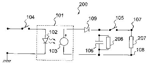
Figure 2 shows the circuit diagram of an exemplary fail-safe
system 200 according to the invention, applied to the detection of current
leaks in a circuit under test that is not represented, connected in parallel
with
a capacitor 106. This circuit under test usually behaves as an open circuit.
Figure 2 differs from figure 1 in that a resistor 208, in parallel with the
capacitor 106, represents the current leakage resistance in the circuit under
test. Furthermore, the input terminals 107 and 108 are connected to a current
measuring device 207. The operation of the system can be broken down into
two distinct phases described hereinbelow:
- A first phase of charging the capacitor 106. In this first phase,
the duration of which is predetermined to ensure that the capacitor
106 is fully charged, the first switch 104 is closed and the second
switch 105 is open. The capacitor 106 is charged, in the same way
as previously described with reference to figure 1. This time, if a
leak is present in the circuit under test, the leak resistance 208
absorbs a portion of the electrical power, and the capacitor 106
can be charged only partially.
- A second phase of discharging the capacitor 106. In this
second phase, the first switch 104 is open and the second switch
105 is closed; thus, the capacitor 106 is discharged into the
measuring device 207. This device can, for example, comprise
means for measuring the voltage at the terminals of the capacitor
106, or even means for measuring a capacitor discharge time, or
even a time at the end of which the voltage at the terminals of the
CA 02685651 2009-11-16
7
capacitor passes below a predetermined threshold. Obviously,
other means of estimating the charge of the capacitor can be
envisaged.
Figure 3A shows the circuit diagram of a fail-safe system 300
according to the invention, applied by way of example to the detection of leak
currents in a switch 310 of N-channel MOSFET type. A first photovoltaic
coupler 320 comprising a light source 321 coupled to a photovoltaic cell 322
is used as energy source for the switch 310. The light emitter 321 is
connected to an energy source via a first switch 305, and to a reference
potential. The positive terminal of the photovoltaic cell 322 is connected to
the gate of the MOSFET switch 310. The negative terminal of the cell 322 is
connected to the drain of the MOSFET switch 310. A second photovoltaic
coupler 101 comprising a light emitter 102 coupled to a photovoltaic cell 103
is used as energy source for charging a capacitor 106. The light emitter 102
is connected to an energy source via a second switch 104, and to the
reference potential. The positive terminal of the photovoltaic cell 103 is
connected to a diode 109. The diode 109 is connected to the source of the
MOSFET switch 310 via a diode 323. The diodes 109 and 323 protect the
photovoltaic cell 103 against returned current. The diode 109 is furthermore
connected to the first armature of a capacitor 106. The negative terminal of
the photovoltaic cell 103 is connected to the second armature of the
capacitor 106. The source of the MOSFET switch 310 is furthermore
connected to an input 311, the drain to an output 312. The drain is
furthermore connected to a current measuring device 313, in this example
consisting of a resistor 314 connected to the primary of a Schmitt trigger
photocoupler 315. The secondary of this photocoupler is connected to a test
output 330. The operation of the system can be broken down into two distinct
phases described hereinbelow:
- In a first phase, the first switch 305 and therefore the MOSFET
switch 310 are open, and the second switch 104 is closed. Thus,
in a manner similar to that described above with reference to
figure 2, the second photovoltaic coupler 101 charges the
capacitor 106, for a predetermined duration to ensure that the
latter is fully charged. Assuming that the MOSFET switch 310
CA 02685651 2009-11-16
8
presents current leaks, the charge of the capacitor 106 can be
only partial.
- In a second phase, the second switch 104 is open and the first
switch 305 is closed. The MOSFET switch 310 is then closed. In
this example, the output 330 is temporarily active, for a duration
dependent on the electric current passing through the resistor 314.
Thus, a leak current in the actuator 310 is reflected in a duration of
the active state of the photocoupler 315 that is less than a
predetermined threshold. Obviously, other types of known devices
able to determine a state of charge of the capacitor 106 can be
envisaged.
Figure 3B is similar to figure 3A. It relates to the case where the
component under test is a P-channel MOSFET type switch 340. The
description given with reference to figure 3A applies to figure 3B, except for
the fact that the positive terminal of the photovoltaic cell 322 of the first
coupler 320 is connected to the source of the MOSFET switch 340. The
negative terminal of the cell 322 is connected to the gate of the MOSFET
switch 340.
Figure 4 shows the circuit diagram of one embodiment of the
invention, applied by way of example to a secured control system comprising
P- and N-channel MOSFET type switches. A system 400 according to the
invention comprises two networks 410 of four modules 401, 402, 403 and
404 fed by a battery and connected to a load 440. The input of the network
410 is connected to the positive terminal of the battery via a disconnecting
relay 412 and a fuse 413. The input of the network 410 is furthermore
connected to two parallel branches, each of them comprising two modules
connected in series. A first parallel branch comprises the first module 401,
in
this example a system comprising a switch of N-channel MOSFET type as
represented in figure 3A, in series with the second module 402, comprising a
P-channel MOSFET type switch as represented in figure 3B, the second
module being mounted in series with a protection diode 420. Two switches
S11 and S12 are connected between the input of the network 410 and the
input of the first module 401. The first switch S11 is connected between the
CA 02685651 2009-11-16
9
input of the network 410 and a terminal of the second switch S12. The other
terminal of the second switch S12 is connected to the negative terminal 414
of the battery. The output of the first module 401 is connected to the input
of
the second module 402. The output of the second module 402 is connected
to a first terminal 430 of the load 440. A second parallel branch comprises
the third module 403, in this example a system comprising a switch of P-
channel MOSFET type as represented in figure 3B, in series with the fourth
module 404, comprising a switch of N-channel MOSFET type as represented
in figure 3A, the fourth module being mounted in series with a protection
diode 420. Two switches S21 and 322 are connected between the input of
the network 410 and the input of the third module 403. The first switch S21 is
connected between the input of the network 410 and a terminal of the second
switch S22. The other terminal of the second switch S22 is connected to the
negative terminal 414 of the battery. The output of the third module 403 is
connected to the input of the fourth module 404. The output of the fourth
module 404 is connected to the first terminal 430 of the load 440. A second
terminal 431 of the load 440 is connected to the input of a second network
410, the output of which is connected to the negative terminal 414 of the
battery. Each of the modules 401, 402, 403 and 404 presents an input 311,
an output 312, a first switch 305 and a second switch 104, and a test output
330, according to the descriptions given with reference to figures 3A and 3B.
Each of these modules is thus able to be tested independently of the other
modules. Thus, any failure of one of the devices forming this system can be
diagnosed rapidly.
Figure 5 shows the circuit diagram of one embodiment of the
invention applied by way of example to the testing of the input of an
electrical
system. Such a fail-safe system according to the invention comprises a
circuit 520 and a test module 510. Advantageously, the test module 510 is
integrated in the circuit 520. The input 521 of the circuit 520 is tested by
the
test module 510. The input 521 is connected to a first switch 524 via a
protection diode 523. The first switch 524 is furthermore connected to a
Zener diode 526. The Zener diode 526 is intended to supply a voltage
threshold to the primary of a Schmitt trigger coupler 527. The secondary of
this coupler is connected to an output 528. The primary of the coupler 527 is
CA 02685651 2009-11-16
linked to a reference potential 522. A line resistance 529 is connected to the
diode 526, just upstream of the latter. A resistor 525 sets the input
impedance. The test module 510 is similar to the systems described above
with reference to the preceding figures. This test module therefore comprises
5 a photovoltaic coupler 101 used as an energy source for charging a capacitor
106. The photovoltaic coupler 101 comprises a light emitter 102 connected to
an energy source via a second switch 104, and to the reference potential.
The light emitter 102 is coupled to a photovoltaic cell 103. The positive
terminal of the photovoltaic cell 103 is connected to a diode 109. The diode
10 109 is connected to the first armature of a capacitor 106. The negative
terminal of the cell 103 is connected to the second armature of the capacitor
106. The latter is furthermore connected to a first terminal of the resistor
525.
The first armature of the capacitor 106 is furthermore connected to the first
terminal of a third switch 501. The second terminal of the switch 501 is
connected to the second terminal of the resistor 525 via a protection diode
502. The operation of the system can be broken down into two distinct
phases described hereinbelow:
- In a first phase, the third switch 501 is open; thus, the test
module 510 is disconnected from the circuit 520. The first switch
524 is closed. Thus, the input 521 is read and transmitted to the
output 528. The second switch 104 is closed, therefore the
capacitor 106 is charged.
- In a second phase, the second switch 104 is open. The first
switch 524 is open, and the output 528 becomes inactive. The
third switch 501 is closed, so the capacitor 106 is discharged into
the circuit 520. The result of this is a pulse on the output 528.
Measuring means, not represented here, can be used to
characterize this pulse. For example, by measuring the duration of
the pulse, it is possible to detect the increase in the resistance
525, and a modification of the input voltage threshold, conditioned
by the Zener diode 526.