Note : Les descriptions sont présentées dans la langue officielle dans laquelle elles ont été soumises.
CA 02695883 2010-03-08
19882EP FB/GK/bb
. .
- 1 -
Computing Device and Start-up Method Therefor
Field of the Invention
The present invention relates to a computing device and to a method of
operating a computing device. In particular, the invention relates to a
computing device with an improved start-up performance.
Background
Computer platforms are implemented in a range of electronic devices,
such as portable electronic devices comprising portable computers,
mobile internet devices, smart phones and the like. Furthermore,
computing platforms are being implemented in vehicles, where they
control a range of vehicle functions. In all these applications it is
desirable that the computing platforms start up quickly, so that the user
is faced with a minimum delay before being capable of operating the
device. Particularly in automotive applications fast start-up times are
required, as the vehicle functions controlled by the computing device
should be available as soon as the vehicle is started. As an example, the
warning sound for reversing the vehicle should become available
immediately after starting the vehicle. Further, there may be special
requirements regarding e.g. early audio and early video.
For the applications mentioned above a computing platform such as the
Intel Centrino AtomTM platform using an Intel AtomTM processor,
which is also termed Menlow or Menlow XL platform, can be employed.
When starting up a computing device, a reset signal is generally supplied
to the central processing unit. When a synchronous reset is used, as it is
CA 02695883 2010-03-08
19882EP FB/GK/bb
- 2 -
the case for the Intel Centrino platform, a clock signal is required for
recognizing and processing the reset signal by the CPU. In conventional
systems, the clock signal is generated by a so-called real-time clock
(RTC), which comprises a 32 kHz quartz oscillator. Such quartz
oscillators have typically an oscillation build-up time of 800 ms or more.
The CPU has to wait for this period of time before being capable of
processing the reset signal. If the reset signal is deactivated before a
valid RTC clock signal is available to the system controller hub of the
computing device, an undefined behaviour will result. Accordingly, the
deactivation of the reset signal needs to be delayed until the oscillation
build-up of the RTC quartz is finalized. An additional delay is thus
introduced in the start-up phase of the computing device. Together with
the delay caused by the initial program load (IPL) and the start-up
application via the relatively slow low pin count (LPC) bus, the delay at a
start-up of such a conventional computing device can no longer meet the
requirements of automotive environments.
A computing system based on such a platform generally requires about
two seconds for starting up, with a system application having a size of
about two megabytes (MB) being loaded during the booting procedure
(IPL). A duration of such a length until the computing device becomes
operable is generally too long for the requirements posed by automotive
applications.
Summary
Accordingly, there is a need for improving the start-up performance of a
computing device. In particular, it is desirable to reduce the time
required by the computing device to become operational.
CA 02695883 2010-03-08
19882EP FB/GK/bb
- 3 -
This need is met by the features of the independent claims. The
dependent claims describe preferred embodiments of the invention.
According to a first aspect of the invention, a computing device
comprising a computing unit and a boot memory is provided. The
computing unit comprises a working memory and a processing unit. The
boot memory comprises control instructions for operating the computing
device which are to be transferred to the computing unit at start-up of
the computing device. The computing device further comprises a boot
control unit interfacing the computing unit by at least a first and a
second interface and interfacing the boot memory by a third interface.
The boot control unit is configured to transfer a first part of the control
instructions from the boot memory via the first interface to the
computing unit and to transfer a second part of the control instructions
from the boot memory via the second interface to the computing unit.
By using two interfaces for transferring the control instructions from the
boot memory to the computing unit, the transfer can be performed
faster, and the time required for a start-up of the computing device can
be reduced.
According to an embodiment of the invention, the second part of the
control instructions is larger than the first part and the second interface
is configured to transfer data at a faster rate than the first interface. The
control instructions are for example part of a boot application which is to
be transferred at start-up of the computing device. As the second part of
the boot application data, which has a larger size, is transferred via the
faster of the two interfaces, the initial program load requires less time,
and the start-up performance is improved accordingly.
CA 02695883 2010-03-08
19882EP FB/GK/bb
= ,
- 4 -
The boot control unit may comprise a direct memory access (DMA)
controller for transferring the second part of the control instructions via
the second interface into the working memory of the computing unit.
Accordingly, the processing unit of the computing unit may not need to
be involved when transferring the second part of the control instructions.
The second part of the control instructions may thus directly be
transferred into the working memory by the DMA controller, e.g. via a
Southbridge or a system controller hub of the computing unit. The
transfer can thus be performed fast and efficiently without the need to
involve the processing unit.
The boot control unit may comprise a field-programmable gate array
(FPGA) or an application-specific integrated circuit (ASIC). With both the
implementation of the boot control unit as a FPGA or as an ASIC, a fast
transfer of the control instructions from the boot memory to the
computing unit via said first and said second interface can be achieved.
The boot control unit may perform a bitwise transfer of the control
instructions, using no buffer or only a small buffer.
The first interface may be a low pin count (LPC) bus. The second
interface may be a peripheral component interconnect express (PCIe)
bus. The third interface between the boot memory and the boot control
unit may be a parallel bus, e.g. an eight bit parallel bus. As only a
smaller part of the control instructions is transferred via the relatively
slow LPC bus, and the larger part of the control instructions is
transferred via the fast PCIe bus, the performance of the initial program
load can be improved significantly.
The first part of the control information may comprise control
instructions for initializing the second interface. The boot control unit
can be configured to transfer the second part of the control instructions
CA 02695883 2010-03-08
19882EP FB/GK/bb
- 5 -
after initialization of the second interface. As an example, the boot
control unit may transfer the first part of the control instructions by the
LPC bus, which is directly available when the computing device is
powered up, in response to which the computing unit initializes the PCIe
bus. After the transfer of the first part and the initialization the second
part of the control instructions is then transferred by the fast PCIe bus.
The computing unit may further comprise a system controller hub (SHC)
which provides the first and the second interface and which interfaces
the working memory. Via the SHC the boot control unit can thus directly
transfer the second part of the control instructions into the working
memory. The SHC may for example be a Poulsbo or Poulsbo XL system
controller hub produced by Intel .
The boot memory may comprise a flash memory. It may be a flash
memory of a relatively small size (e.g. between 4 and 32 MB), such as
about 8 MB or about 16 MB, yet the boot memory may also be part of a
larger memory, such as a hard drive or a memory card. The computing
unit may comprise an Intel Menlow or Menlow XL platform being
provided with the system controller hub mentioned above. The
processing unit may be an X86 compatible microprocessor. In particular,
an Intel AtomTM microprocessor may be used.
According to another aspect of the invention, a method of operating a
computing device is provided, the computing device comprising a
computing unit with a working memory and a processing unit, a boot
memory comprising control instructions for operating the computing
device which are to be transferred to the computing unit at start-up of
the computing device, and a boot control unit interfacing the computing
unit by at least a first and a second interface at interfacing the boot
memory by a third interface. The method comprises the steps of
CA 02695883 2010-03-08
19882EP FB/GK/bb
. .
- 6 -
retrieving the control instructions from the boot memory by the boot
control unit, transferring a first part of the control instructions via the
first interface to the computing unit, and transferring a second part of
the control instructions via the second interface to the computing unit.
The method can be performed at the start-up of the computing device,
e.g. shortly after powering on the computing device. According to an
embodiment, the control instructions are stored in a compressed format
in the boot memory, and the method further comprises the step of
decompressing the control instructions by the processing unit after the
compressed control instructions are received at the computing unit.
The computing device being operated by said method may be configured
as described above.
With the method of operating the computing device the control
instructions can be transferred faster from the boot memory via said two
interfaces to the computing unit, so that the start-up performance of the
computing device is improved.
According to a second aspect of the present invention, a computing
device comprising a computing unit with a system controller, a working
memory, and a processing unit is provided, the system controller
comprising a clock interface for receiving a clock signal, wherein the
system controller is further configured to provide a received clock signal
and a reset signal to the processing unit at start-up of the computing
device. The processing unit is configured to use the provided clock signal
for processing the reset signal. The computing device further comprises a
system management controller (SMC) interfacing the clock interface of
the system controller, wherein the system management controller is
CA 02695883 2010-03-08
19882EP FB/GK/bb
. .
- 7 -
adapted to supply a clock signal to the system controller via the clock
interface.
In conventional computing devices the clock signal is generally provided
by a real-time clock (RTC), which comprises a quartz crystal oscillator
running at 32 kHz and requiring a substantial amount of time for
oscillation build-up. By supplying the clock signal of the system
management controller to the computing unit, the time required for
recognizing a reset signal and accordingly the time required for starting
up the computing device can be reduced.
According to an embodiment, the computing device further comprises an
electronic oscillator for generating the clock signal, the electronic
oscillator being connected to the system management controller. The
electronic oscillator may for example be a quartz crystal oscillator
operating at a frequency substantially higher than the 32 kHz at which a
conventional RTC oscillator is operated. Accordingly, the oscillation
build-up occurs much faster, and the clock signal becomes available a
short time after turning on the computing device, e.g. within 10 to 50
ms.
The electronic oscillator may comprise a quartz crystal oscillator and
may generate the clock signal with a frequency above 1 MHz, wherein
the system controller may be adapted to operate with a clock signal
having a frequency below 1 MHz. The electronic oscillator may for
example operate in a range between 1 MHz and 1 GHz, wherein the
system controller may require a clock signal in a range between 10 and
100 kHz, e.g. 32.8 kHz.
The system management controller may comprise a frequency divider
adapted to divide a frequency of the clock signal generated by the
CA 02695883 2010-03-08
19882EP FB/GK/bb
- 8 -
electronic oscillator, so as to adapt the frequency of the clock signal to a
frequency required by the system controller. That way, a high frequency
oscillator with a fast oscillation build-up can be used, while the system
controller can still be provided with a clock signal of the correct
frequency.
The system controller may be a system controller hub (SCH), such as the
Poulsbo or Poulsbo XL system controller hub produced by Intel . As
mentioned above, the computing unit may comprise an Intel Menlow or
Menlow XL platform, and the processing unit may be an X86 compatible
microprocessor. The SMC may be a small version of input/output (I/O)
controller or an integrated combined chip including an I/O controller
function, a power supply function and a system clock function.
The computing device according to the second aspect of the invention
may further be configured as mentioned above with respect to the first
aspect of the invention. In particular, it may comprise a boot control unit
interfacing a boot memory and interfacing the computing unit via at
least a first and a second interface for transferring control instructions
stored in the boot memory partly via the first and via the second
interface to the computing unit.
According to a further aspect of the invention, a method of operating a
computing device comprising a computing unit, which comprises a
system controller, a working memory and a processing unit is provided.
The system controller comprises a clock interface for receiving a clock
signal, and the computing device further comprises a system
management controller (SMC) interfacing the clock interface of the
system controller. The method comprises the steps of supplying a clock
signal from the system management controller to the system controller
via the clock interface at start-up of the computing device, providing, by
CA 02695883 2010-03-08
19882EP FB/GK/bb
. ,
- 9 -
the system controller, the received clock signal and a reset signal to the
processing unit and, at the processing unit, using the provided clock
signal for processing the reset signal.
The advantages outlined above with respect to the device according to
the second aspect of the invention may also be achieved by this method.
In particular, as the clock signal from the system management controller
is available already a short time after powering on the computing device,
the recognition of the reset signal at the system controller and the
processing unit and the resetting of the reset signal can be performed
faster.
According to an embodiment, the method further comprises generating
the clock signal by an electronic oscillator or quartz connected to the
system management controller and dividing a frequency of the clock
signal generated by the electronic oscillator or quartz in said system
management controller so as to adapt the frequency of the clock signal
to a frequency required by the system controller.
The method may further comprise providing the reset signal from the
system management controller to the system controller and deactivating
the reset signal after the reset signal is being processed by the
processing unit. As the deactivation of the reset signal may be performed
faster by the above method, the time required for starting up the
computing device can be reduced.
Furthermore, the computing device may be configured as described
above with respect to the first and/or the second aspect of the invention.
In particular, the computing device may further be configured as
described above with respect to the first aspect of the invention, and the
method may further comprise the steps of one of the methods described
CA 02695883 2010-03-08
19882EP FB/GK/bb
- 10 -
with respect to the first aspect of the invention. As an example, after
performing the reset operating mentioned above, the method may further
comprise the transferring of control instructions from a boot memory via
a first and a second interface to the computing unit by means of a boot
control unit. By a combination of these methods, the time required for
starting up the computing device can further be reduced. The
improvement in start-up performance may enable the computing device
to meet the system start-up requirements of automotive applications.
The features of the above aspects and embodiments of the invention may
be combined with each other unless noted to the contrary.
Brief Description of the Drawings
The foregoing and other features and advantages of the invention will
become further apparent from the following detailed description read in
conjunction with the accompanying drawings. In the drawings like
reference numerals refer to like elements.
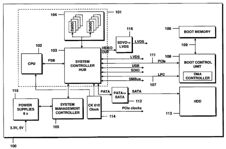
Fig. 1 is a schematic block diagram illustrating a computing device
according to an embodiment of the present invention.
Fig. 2 is a flow diagram illustrating a method according to an
embodiment of the present invention.
Fig. 3 is a flow diagram illustrating an embodiment of a method
according to the second aspect of the invention.
Fig. 4 is a flow diagram illustrating an embodiment of a method
according to the first aspect of the invention.
CA 02695883 2010-03-08
19882EP FB/GK/bb
. .
- 11 -
Detailed Description
It is to be understood that the following description of embodiments is
given only for the purpose of illustration and is not to be taken in a
limiting sense. It should be noted that the drawings are to be regarded
as being schematic representations only, and elements in the drawings
are not necessarily to scale with each other. Rather, the representation
of the various elements is chosen such that their function and general
purpose become apparent to a person skilled in the art. The partitioning
of embodiments in function blocks or units shown in the drawings is not
to be construed as indicating that these units necessarily are
implemented as physically separate units, but functional blocks or units
shown or described may be implemented as separate units, circuits,
chips or circuit elements, but one or more functional blocks or units may
as well be implemented in a common circuit, chip, circuit element or
unit.
The schematic block diagram of Fig. 1 shows a computing device 100
which comprises a computing unit 101. Computing unit 101 comprises a
central processing unit 102, a system controller hub 103 and a working
memory 104. In the embodiment of Fig. 1, the computing device 100 is
based on an Intel Centrino AtomTM platform, in particular on a
Menlow or Menlow XL platform, and the system controller hub 103 is a
Poulsbo or Poulsbo XL controller hub. CPU 102 is an Intel AtomTM
processor. It should be clear that other platforms comprising different
processors and system controllers may also be used with the present
invention. Memory 104 comprises plural double data rate 2 (DDR2)
random access memory (RAM) modules, yet it may also comprise other
types of memory.
CA 02695883 2010-03-08
19882EP FB/GK/bb
- 12 -
Computing device 100 further comprises system management controller
(SMC) 105. SMC 105 may control functions such as power flow and fan
speed. In the present embodiment it is also used to signal a reset event
to the computing unit 101. It may for example be signalled to the SCH
103 and other components of the platform requiring a reset signal. SMC
105 may comprise clock 114 and power supply 115 and may be
implemented in one combined chip solution.
When starting the computing device 100, the first start-up phase is
generally controlled by hardware. The phase comprises the recognition of
the reset signal, which is controlled by the availability of a valid clock
signal for the synchronous reset interface. Without the clock signal, the
reset signal cannot be processed by computing unit 101.
In conventional systems, a real-time clock quartz is used for generating a
clock signal at a frequency of e.g. 32.8 kHz, yet such a RTC quartz
requires an oscillation build-up time of more than 800 ms. Such high
oscillation build-up times are in particular encountered in automotive
environments, where batteries may not be used for running the RTC
quartz.
The present embodiment of Fig. 1 does not use a clock signal from a RTC
quartz, but uses a clock signal from the SMC 105. SMC 105 may itself
comprise a quartz oscillator, or may interface an oscillator external to
SMC 105 (not shown in Fig. 1). The quartz oscillator connected to SMC
105 operates at a higher frequency than the RTC quartz, e.g. in the MHz
range. As a result, the oscillation build-up time of the oscillator
connected to SMC 105 is shorter than that of a RTC quartz, it may be as
short as 10 to 20 ms. System management controller 105 comprises one
or more frequency dividers which reduce the frequency of the clock
signal. The SCH 103 may still require a clocking signal with a frequency
CA 02695883 2010-03-08
19882EP FB/GK/bb
- 13 -
of 32.768 kHz, which is the frequency generally produced by the crystal
oscillator of a RTC. SMC 105 adapts the frequency of the clock signal to
this frequency required by the SCH 103.
As the clock signal provided by SMC 105 to SCH 103 is available much
earlier than the clock signal of a conventional RTC, SCH 103 can start
processing the reset signal much earlier, and the time span to the
deactivation of the reset signal can be significantly reduced. SCH 103
provides both the reset signal and the clock signal to CPU 102 at start-
up. During the operation of computing device 100, SMC 105 continues
to supply the clock signal to SCH 103.
As SMC 105 generates the reset signal, it needs to be supplied with the
RTC clock signal in a conventional system. As in the present
embodiment the SMC 105 generates the clock signal itself, such a
feedback of the RTC clock signal to the SMC 105 is not required in the
present embodiment.
After the start-up phase described above, a further initialization of
computing device 100 may be performed according to any method known
in the art. This may comprise an initialization of memory 104, and the
like.
The start-up of computing device 100 further requires the loading of
control instructions into computing unit 101. Such a boot code or boot
application comprising these control instructions is stored in boot
memory 106, which is implemented as a flash memory in the present
embodiment. The loading of the boot code during the start-up of the
computing device 100 may also be termed "initial program load" (IPL). In
conventional computing devices, the loading process of the boot code is
performed via the relatively slow low pin code (LPC) bus 107, which
CA 02695883 2010-03-08
19882EP FB/GK/bb
, .
- 14 -
achieves a speed of approximately 2 MB per second and is directly
connected to a flash memory unit with a LPC interface. The time
required for loading the boot application is thus determined by the
bandwidth of the LPC interface 107 in conventional systems.
In the embodiment of Fig. 1, a boot control unit 108 is provided, which
interfaces the boot memory 106 via a parallel interface 109. This may for
example be an 8 bit interface. The boot control unit 108 is a field-
programmable gate array (FPGA) or an application-specific integrated
circuit (ASIC). Both of these units can be configured for performing
specified functions fast and efficiently. Boot control unit 108 can for
example be configured so as to comprise a direct memory access (DMA)
controller 110. Boot control unit 108 interfaces the SCH 103 via a LPC
bus 107 and via a PCIe bus 111. The PCIe bus 111 provides a data
transfer rate that is significantly higher than that of the LPC bus 107.
Yet the PCIe interface 111 is generally not available at the start-up of the
computing device 100, as it has to be initialized.
Boot control unit 108 thus accesses boot memory 106 and transfers a
first part of the control instructions stored thereon via LPC bus 107 to
SCH 103. These instructions are executed and initialize the PCIe
interface 111. During this initial boot, e.g. 100-300 kB of boot code may
be transferred to SCH 103. After the initial boot, the boot control unit
108 switches to the PCIe interface 111. Due to the much higher
bandwidth of the connection between the boot memory 106, the boot
control unit 108 and the SCH 103 via parallel interface 109 and PCIe
interface 111, the remaining part of the boot code can be transferred at a
much higher rate than possible via a standard LPC bus. As an example,
when using a boot code with a size of 2 MB, the transfer is about 900 ms
faster as compared to loading the data directly from the boot flash via a
LPC bus. The boot data may also be loaded from other DMA-capable
CA 02695883 2010-03-08
19882EP FB/GK/bb
. .
- 15 -
mass storage devices, such as a hard drive, a SD card or other types of
memory cards, and the like, which may have latencies on the order of
several hundreds of milliseconds. Compared to loading the data from a
secure digital (SD) card via a LPC bus, the computing device of the
present embodiment still achieves a 300 ms faster loading of the boot
data from the boot flash 106.
As mentioned above, the boot control unit 108 may be implemented as
an ASIC or a FPGA. Compared to the realization using a FPGA, which
itself requires a certain time for initialization, the ASIC loading times are
about 150-300 ms shorter.
All or part of the control instructions may be provided as a compressed
boot image in boot memory 106. During the DMA-transfer of the boot
image via PCIe 111 the central processing unit 102 may decompress the
boot image data. The decompression can be performed relatively fast, so
that shortly after the boot image is transferred to memory 104 the
corresponding data is available in a decompressed format.
By providing the RTC clock signal required for the reset by the system
management controller 105 and by transferring the boot application via
both LPC bus 107 and PCIe bus 111, the computing device 100 of the
present embodiment can achieve an improvement in start-up
performance of about 500-1000 ms or even more. The time required for
starting up computing device 100 can thus be halved. As a result,
computing device 100 is capable of meeting the stringent requirements
posed on computing devices for automotive applications.
It should be clear that in other embodiments SCH 103 may receive the
clock signal from a standard RTC clock, while the control instructions
required for booting device 100 are transferred as described above. In
CA 02695883 2010-03-08
19882EP FB/GK/bb
, .
- 16 -
other embodiments, a standard boot procedure may be implemented,
e.g. by transferring the boot application from the boot memory only via a
LPC bus, while the clock signal is provided by the SMC 105 as described
above. Such embodiments will also provide an improved start-up
performance compared to conventional computing devices, yet the device
of Fig. 1 will achieve an even better performance.
The computing device 100 may comprise further components that are
common to conventional computing devices. Such components are
known to the person skilled in the art and will thus not be described in
greater detail here. Examples include a serial advanced technology
attachment (SATA) interface 112 and a connected hard disk drive (HDD)
113, a clock 114 for generating further clock signals, and a power supply
115 supplying power to the computing device 100. Clock 114 may for
example be used for providing a clock signal to CPU 102 and to PCIe
components. Note that clock 114 provides a clock signal different from
the clock signal required for processing the reset signal at start-up of the
computing device 100. The clock signal supplied by SMC 105 and used
when processing the reset signal may also be provided throughout the
operation of computing device 100.
Further, a video output is provided and a converter 116 for converting
the serial digital video out (SDVO) signal into a low voltage differential
signal (LVDS). The signal may be supplied to a display. It should be clear
that some of the components shown in Fig. 1 are optional, such as units
112-116 and the further LVDS, USB, SDIO and SM busses.
Computing device 100 may for example be implemented as a control unit
for a vehicle. It may for example control light, sound or engine-related
functions of the vehicle. Yet computing device 100 may also be
implemented in other devices, such as portable computing devices, e.g. a
CA 02695883 2010-03-08
19882EP FB/GK/bb
- 17 -
portable computer, a smart phone, a mobile internet device, a personal
digital assistance and the like. Other implementations will suggest
themselves to those skilled in the art and the scope of the invention is
not limited to the implementations mentioned above.
Fig. 2 shows a flow diagram of a method according to an embodiment of
the invention. The method may be implemented on the computing device
100 shown in Fig. 1. The method comprises powering up the computing
device (step 200) and performing a reset operation (step 300). The reset
operation 300 is described in more detail further below with respect to
Fig. 3. In step 400, an initial program load is performed. The initial
program load is described in more detail further below with respect to
Fig. 4. After these start-up operations, the computing device is
operational and can be operated in step 500, in accordance with its
specified functionality.
It should be clear that the start-up procedure shown in Fig. 2 can
comprise further steps common to start-up procedures of computational
devices. Such additional steps may comprise further initialization
phases, such as initializing the chip set of the computing device, e.g.
comprising northbridge and southbridge, performing a memory
initialization and the like. Such procedures are known to the skilled
person and will not be described in further detail here.
Fig. 3 shows a flow diagram of a method according to an embodiment of
the second aspect of the present invention. In step 301, the electronic
oscillator connected to the SMC 105 is started to generate a clock signal.
In the SMC 105, a frequency division is performed to adapt the
frequency of the clock signal to the frequency required by the SCH 103
(step 302). In step 303, a reset signal is supplied from the SMC 105 to
the SCH 103. Further, the clock signal generated by frequency division
CA 02695883 2010-03-08
19882EP FB/GK/bb
- 18 -
in SMC 105 is supplied to the system controller hub 103 in step 304.
SCH 103 supplies the reset signal (step 305) and the clock signal (step
306) to the processing unit 102. Note that the order of providing the
reset signal and the clock signal to the SCH and to the processing unit
may be different, e.g. reversed. These signals can be supplied
asynchronously. The recognition of the reset generally occurs after a
certain number of clock cycles. The recognition of the reset signal can
thus occur synchronously. As the clock signal from SMC 105 is available
shortly after powering up the computing device 100, the CPU 102 can
start to process the reset signal with a very short delay (step 307).
The reset signal is then deactivated in step 308. Compared to systems
which use a clock signal from a real-time clock for processing the reset
signal, the reset signal can be deactivated several hundred microseconds
earlier. After the reset signal is deactivated, the start-up procedure of the
computing device 100 is continued (step 309).
Fig. 4 is a flow diagram of a method according to an embodiment of the
first aspect of the present invention. In step 401, the boot control unit
108 accesses a first part of the control instructions stored on the boot
memory 106. The boot control unit 108 transfers the first part of the
control instructions to the computing unit 101 via the LPC bus 107. In
the embodiment of Fig. 1, the instructions are transferred to the SCH
103, although it should be clear that other controllers or units may used
for providing the LPC interface. The transfer may for example occur
bitwise without the need to buffer larger parts of said control
instructions in the boot control unit 108. The first part of the control
instructions may for example comprise 100-300 kB of data. In step 403,
the first part of the control instructions is processed, e.g. by SCH 103
and CPU 102. As a result of the processing, the PCIe bus 111 is
initialized in step 104. After initialization of the PCIe bus, the transfer of
CA 02695883 2010-03-08
19882EP FB/GK/bb
- 19 -
the boot application is switched over to the PCIe bus. Accordingly, the
boot control unit transfers a second part of the control instructions from
the boot memory 106 to the computing unit 101 via the PCIe bus 111
(step 405). The transfer of the second part of the control instructions can
be controlled by the DMA controller 110 and can occur directly (i.e. via
SCH 103) into the memory 104 of computing unit 101. If the control
instructions are stored in a compressed format in boot memory 106, the
CPU 102 may decompress the data during the DMA transfer (step 406).
As the decompression can be performed in parallel to the data transfer,
the decompression results in a negligible delay. After the boot
application is loaded into the memory 104, the computing device 100
can operate according to these control instructions (step 407). The
control instructions may as such comprise a basic operating system of
the computing device 100.
The methods described with respect to Figs. 3 and 4 may comprise
further steps which are commonly performed during the system reset or
during the loading of the boot application, respectively. The steps may
also be performed in different orders or in parallel. For example, the
generation and supplying of the clock signal to the SCH in step 304 and
the supplying of the reset signal to the SCH in step 305 may be
performed in parallel.
In summary, the present invention provides an improved start-up
performance of a computing device. The improvements that can be
achieved with the present invention are such that the computing device
can be employed for automotive applications, as it is capable of meeting
the requirements set for such environments.
While specific embodiments of the invention are disclosed herein, various
changes and modifications can be made without departing from the
CA 02695883 2012-07-17
19882EP FB/GK/bb
- 20 -
scope of the invention. The present embodiments are to be considered in
all respects as illustrative and non-restrictive, and the scope of the
claims should not be limited by the preferred embodiments set forth in
the examples, but should be given the broadest interpretation consistent
with the description as a whole.