Note : Les descriptions sont présentées dans la langue officielle dans laquelle elles ont été soumises.
CA 02750437 2011-08-25
246129
THERMAL INTERFACE MATERIAL FOR REDUCING THERMAL
RESISTANCE AND METHOD OF MAKING THE SAME
BACKGROUND OF THE INVENTION
The subject matter described herein relates generally to a themial interface
material,
and, more particularly, a thermal interface material for reducing thermal
resistance
between a circuit card assembly (CCA) and a chassis.
Enclosures designed to remove heat from a CCA by way of thermal conduction,
such
as those assemblies containing high power devices, are increasingly challenged
to
remove higher levels of heat. This is because newly developed processing
devices
typically contain more circuitry and therefore tend to generate higher heat
loads, or
because components are smaller, thus permitting a CCA to contain more
components,
thereby increasing an amount of heat generated per CCA.
Various systems have been devised for pressing, via a board retainer, opposite
edges
of the thermal interface of a CCA to a chassis which acts as a heat sink to
carry away
heat generated by CCA components on opposite sides of the thermal interface.
However, currently, a thermal interface between a CCA and a chassis is metal
to
metal without a thermal intermediate material between the two metals. The
metal to
metal interface is poor thermally, with a typical difference in temperature
(AT) in the
order of 10 C from the thermal interface of a CCA to a cold wall of a chassis.
While
a metal to metal interface may be sufficient where CCA wattage is low, new
designs
of CCAs are dissipating progressively more heat as electronic devices become
smaller
and/or operate at higher speeds, rendering the metal to metal interface
inadequate. As
such, heat transferability breaks down or is insufficient, and performance of
an
electronic device in which they are used is adversely affected.
CA 02750437 2011-08-25
246129
BRIEF DESCRIPTION OF THE INVENTION
In one aspect, a thermal interface is provided. The thermal interface material
includes
a thermally conductive metal having a first surface and an opposing second
surface, a
diffusion barrier plate coupled to the first surface of the thermally
conductive metal
and the second surface of the thermally conductive metal, and a thermal
resistance
reducing layer coupled to the diffusion barrier plate.
In another aspect a system is provided. The system includes a circuit card
assembly,
and a housing including a slot having an upper surface and lower surface. The
slot is
configured to receive the circuit card assembly between the upper surface and
the
lower surface. A shim is configured to reduce thermal resistance. The shim is
coupled between the circuit card assembly and the upper surface of the slot. A
board
retainer secures the shim between the circuit card assembly and the upper
surface of
the slot.
In yet another aspect a method of forming a thermal interface material is
provided.
The method includes providing a layer of copper, providing a layer of nickel
over the
layer of copper, and providing a layer of indium over the layer of nickel.
BRIEF DESCRIPTION OF THE DRAWINGS
The present disclosure is described in detail below with reference to the
attached
drawing figures.
Figure 1 shows a sectional end view of a CCA located in the cold wall of a
chassis.
Figure 2 is a sectional view of an exemplary thermal interface material taken
along
sectional line 2-2 shown in Figure 4.
Figure 3 is a sectional view of an alternative thermal interface material.
Figures 4 and 5 show exemplary adhesive applications to a surface of a thermal
interface material.
-2-
CA 02750437 2011-08-25
246129
Figure 6 is a flow chart of an exemplary process of fanning a thermal
interface
material.
Figure 7 shows a plurality of shims etched from a copper foil frame.
DETAILED DESCRIPTION OF THE INVENTION
Although the present disclosure describes a thermal interface material (TIM)
between
a circuit card assembly (CCA) and a chassis, aspects of the disclosure are
operable
with any apparatus that performs the functionality illustrated and described
herein, or
its equivalent. For example, and without limitation, the TIM described herein
may be
placed between a power supply unit and a base plate, a chassis and cooling
fins, a
chassis and a base plate, and the like.
Current thermal interfaces between a CCA and a chassis are metal to metal and
do not
include a TIM between the two metals. However, as mentioned above, a metal to
metal interface may be sufficient where the overall CCA wattage is low. New
designs
of CCAs using electronic devices which are becoming smaller and/or operate at
higher speeds emit a greater amount of energy and heat, rendering a metal to
metal
interface inadequate. For example, high performance conduction cooled CCAs are
expected to run continuously with a temperature at a cold wall interface at 85
C
(typically, a processor manufacturer specifies an upper junction temperature
limit of
105 C). This leaves a difference in temperature (AT) of 20 C between a
processor
and a cold wall thermal interface. Trials of conventional CCAs with a 40 watt
load on
one of the two CCA metal to metal interfaces resulted in a AT of 7.9 C across
the
metal to metal interface. This gives an approximate thermal resistance of 0.2
C/W
across the interface. Thus, a CCA with a maximum load of 160 watts (80 watts
per
interface) would increase the AT to approximately 16 C, which may be
problematic.
However, unlike conventional systems that include, for example, a metal to
metal
interface between a CCA and a chassis and are only sufficient where a CCA
wattage
is limited, the TIM described herein reduces a thermal resistance at an
interface by at
least a factor of 10, and thus may be applied to a CCA with a load lower than
20
watts, as well as a CCA with a load greater than 160 watts.
-3-
CA 02750437 2011-08-25
246129
With reference now to Figure 1, an end view of a housing (e.g., a chassis 102)
for a
CCA is shown. Chassis 102 includes cold walls 104 and 106 that form a slot 108
extending along a length of cold walls 104 and 106. Slot 108 has an upper
surface
110 (e.g., a bottom surface of cold wall 104) and a lower surface 112 (e.g.,
an upper
surface of cold wall 106). A board retainer, or any other suitable fixing
mechanism,
such as a wedgelock 114, is coupled between cold walls 104 and 106 and abuts
lower
surface 112. A CCA 116, and more specifically, a thermal interface surface 117
of
CCA 116, is placed between an upper surface 118 of wedgelock 114 and upper
surface 110 of slot 108. A TIM 120 (e.g., a shim) configured to reduce thermal
resistance is coupled between thermal interface surface 117 and upper surface
110 of
slot 108. Thermal interface surface 117 and TIM 120 are compressed between
upper
surface 110 of slot 108 and upper surface 118 of wedgelock 114. As described
in
further detail below, TIM 120 includes a plurality of layers. In some
embodiments,
each layer of the plurality of layers may include two or more layers.
In certain embodiments, wedgelock 114 is a mechanical fastener designed to
secure
CCA 116 and TIM 120 in slot 108 by expanding and applying contact pressure
between CCA 116 and upper surface 110 of cold wall 106, via a plurality of
individual wedges (not shown). For example, wedgelock 114 mechanically secures
CCA 116 and TIM 120 in slot 108 by expanding the plurality of wedges using an
expansion screw (not shown) and causing pressure to be applied between CCA 116
and upper surface 110 of slot 108.
TIM 120 conforms between two mating surfaces, thermal interface surface 117
and
upper surface 110 of slot 108, and possesses a low bulk thermal resistance and
low
contact resistance. As will be described in greater detail below, to optimize
thermal
performance, TIM 120 includes an interface material and/or interface layer
(e.g.,
indium) and is able to conform to non-planar surfaces and thereby lower
contact
resistance. TIM 120 also possesses a high thermal conductivity and a high
mechanical compliance, yielding elastically when force is applied to TIM 120.
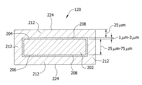
With reference now to Figure 2, a sectional view of an exemplary TIM (e.g.,
TIM
120) is shown. TIM 120 includes a thermally conductive metal 202 having a
first
-4-
CA 02750437 2011-08-25
246129
surface 204 and an opposing second surface 206, a diffusion barrier plate 208
that
circumscribes (e.g., wraps around) thermally conductive metal 202, and a
thermal
resistance reducing layer 212 that circumscribes diffusion barrier plate 208.
As mentioned above, a suitable TIM should conform between two mating surfaces,
as
well as possess a low bulk thermal resistance and low contact resistance.
Thus,
thermal resistance reducing layer 212 includes a conforming metal, such as
indium.
However, due to the soft nature of indium, TIM 120 is layered with other
metals to
provide a more solid TIM while maintaining conductivity. For example,
thermally
conductive metal 202, such as copper, is provided as a stiffener, which
enables TIM
120 to maintain a more solid form. However, due to the diffusing nature of
copper
and indium, nickel plating (e.g., diffusion barrier plate 208) acting as a
diffusion
barrier is provided between thermally conductive metal 202 (e.g., the copper
layer)
and thermal resistance reducing layer 212 (e.g., the layer of indium).
In some embodiments, thermal resistance reducing layer 212 has a thickness of
about
25 microns (p.m), thermally conductive metal has a thickness of about 25 pm
thick to
about 75 m, and diffusion barrier plate 208 has a thickness of about 1 p.m to
about 3
pm.
With reference now to Figure 3, an alternative TIM 320 is shown. TIM 320
includes
a first thermal resistance reducing layer 312 coupled to a first diffusion
barrier plate
308 and a second thermal resistance reducing layer 314 coupled to a second
diffusion
barrier plate 310. In this embodiment, first thermal resistance reducing layer
312 and
second thermal resistance reducing layer 314 are separated by thermally
conductive
metal 202, first diffusion barrier plate 308, and second diffusion barrier
plate 310.
In some embodiments, an adhesive layer 222 is applied to at least one outer
surface
224 of TIM 120. However, a complete surface layer of an adhesive may impede a
flow of heat through TIM 120 and thus increase a thermal resistance of TIM
120.
Thus, adhesive layer 222 may be applied to TIM 120 in a striped pattern, as
shown in
Figure 4, or an array/grid pattern, as shown in Figure 5. Further, an adhesive
layer
that is too thick may impede TIM 120 from properly conforming to thermal
interface
surface 117 of CCA 116 or upper surface 110 of cold wall 106. Thus, in some
-5-.
CA 02750437 2011-08-25
246129
embodiments, adhesive layer 222 includes a layer of adhesive that has a
thickness of
about 5 pm to about 25 pm.
In some embodiments, adhesive layer 222 is used to temporarily attach TIM 120
to
thermal interface surface 117, prior to TIM 120 being secured between CCA 116
and
upper surface 110 of cold wall 106 via wedgelock 114. Further, because
adhesive
layer 222 is sacrificial, adhesive layer 222 includes a low tack adhesive that
enables
TIM 120 to be easily removed from CCA 116 and upper surface 110 of cold wall
106,
leaving thermal interface surface 117 clean for a replacement TIM.
With reference now to Figure 6, a flow chart of an exemplary process of
forming a
TIM is shown, and referenced generally as process 500. Process 500 includes
providing a layer of copper at 502, providing a plated layer of nickel over
the layer of
copper at 504, and providing a plated layer of indium over the plated layer of
nickel at
506. In some embodiments, the plated layer of nickel is provided such that the
plated
layer of nickel circumscribes the layer of copper. In further embodiments, the
plated
layer of indium is provided such that the plated layer of indium circumscribes
the
plated layer of nickel. In other embodiments, a first plated layer of nickel
is provided
over a first surface of the layer of copper, and a second plated layer of
nickel is
provided over an opposing second side of the layer of copper. In other
embodiments,
a first plated layer of indium is provided over the first plated layer of
nickel and a
second plated layer of indium is provided over the second plated layer of
nickel, with
each of the first plated layer of indium and the second plated layer of indium
being
separated by the first plated layer of nickel, the layer of copper, and the
second plated
layer of nickel.
In some embodiments, a plurality of shims 602 are chemically etched from, for
example, 37.5 gm copper foil and held in a frame 604 by tabs 606 (see Figure
7). As
such, shapes, sizes, and holes can be easily accommodated by simply altering
the
photowork. Shims 602 can also be laser cut, enabling shapes, sizes, and holes
to be
changed via software. After shims 602 are etched, frame 604 is preconditioned
for
plating. A layer of nickel (e.g., approximately 3 pm thick) is plated onto all
surfaces
of shims 602 to act as a barrier between copper and indium as indium readily
diffuses
-6-
CA 02750437 2016-08-19
246129
=
into copper resulting in a hard brittle alloy. Next, a layer
of indium (e.g.,
approximately 25 m to about 30 um thick) is plated over the nickel barrier.
Next, adhesive layer 222 may be applied to at least one side of the plurality
of shims
602. A tack adhesive may come in reel form on a backing sheet, and thus, the
adhesive can either be laser cut to produce a striped pattern or an array/grid
pattern (as
shown in Figures 4 and 5, respectively) or a thin mask can be cut which lays
over the
reel of the tack adhesive exposing an array/grid pattern or a striped pattern.
The
adhesive layer is laid onto each of the plurality of shims 602 by hand with a
backing
sheet left in place to protect the tack adhesive. One of ordinary skill in the
art will
appreciate that this process can be automated if quantities permit. Finally,
the plurality
of shims 602 can either be left on frame 604 or cut out as required.
This written description uses examples to disclose the invention, including
the best
mode, and also to enable any person skilled in the art to practice the
invention,
including making and using any devices or systems and performing any
incorporated
methods. The patentable scope of the invention may include other examples that
occur
to those skilled in the art in view of the description. Such other examples
are intended
to be within the scope of the invention described.
=
-7-