Note : Les descriptions sont présentées dans la langue officielle dans laquelle elles ont été soumises.
CA 02768873 2012-01-23
WO 2011/009209 PCT/CA2010/001139
NANOFLUIDIC CELL
CROSS-REFERENCE TO RELATED APPLICATION
This application claims priority to U.S. Provisional Application No.
61/227,893 titled "NANOFLUIDIC CELL" and filed on July 23rd, 2009, the
entire contents of which are incorporated herein by reference.
FIELD OF THE INVENTION
The present invention relates to devices and methods for the analysis
of nanoliter or sub-nanoliter fluid volumes via analytical methods including
electron, x-ray, and optical characterization.
BACKGROUND OF THE INVENTION
Microscopy and materials characterization methods typically employ
light, electrons, acoustic waves and other forms of electromagnetic radiation
to investigate optical, electronic and/or structural properties of a sample of
interest.
Electron microscopy is among the most powerful tools in resolving
structure at the atomic level. Unlike its optical counterpart that is limited
by
the wavelength of visible light, electron microscopy utilizes electrons in the
range of 10 keV to 1 MeV to probe matter. In this energy range, electrons
have sub-angstrom wavelength and are therefore capable of directly imaging
atomic arrangements, yielding a magnification power of up to approximately
1
CA 02768873 2012-01-23
WO 2011/009209 PCT/CA2010/001139
106. Unfortunately, the penetration depth of electrons, by virtue of their
high
scattering cross-section, is limited to 100 nm length scales or less. Samples
must be prepared with thickness of nanoscale dimensions such that sample
preparation is a major component to the art of electron microscopy.
In addition to electron microscopy, there are important applications
where the penetration of the probing interaction is so small that it has been
impossible to study strongly absorbing samples. The application of soft x-
rays for structural analysis also involves absorption depths on the 100 nm
scale. Similar probes arise in the use of infrared probes of molecular
vibrations in liquids. This problem is particularly severe for electrons where
one would like to image biological samples under aqueous conditions.
Sample path-lengths, including windows, are preferably kept under the 100
nm scale. Consequently the use of an electron microscope demands
preparing thin samples.
Such a constraint essentially limits the application of electron probes
and other powerful tools of structure to studying samples in the solid phase
where structural rigidity permits 100 nm thick sections. However, even in this
case, there are important limitations. For example, to determine the structure
of a protein using electron diffraction, one has to first crystallize the
protein
and subsequently prepare a stable thin film from the crystal. The
crystallization process involves a certain degree of dehydration of the
sample,
and is thought to alter the structure of the protein to be investigated.
2
CA 02768873 2012-01-23
WO 2011/009209 PCT/CA2010/001139
Ideally, one would like to study systems in their natural environment.
Since most biological systems occur in solution, one would ultimately like to
directly probe liquids without any manipulation that causes denaturation,
evaporation or other degradation of the sample. A solid structure that is
capable of confining samples to nano-scale thicknesses yet allowing
electrons or radiation to penetrate the structure is therefore needed.
SUMMARY OF THE INVENTION
The present invention addresses this need by providing a flow cell that
enables the probing of fluid samples. Furthermore, the flow cell is adapted
for
use with optical, x-ray, acoustic and electron analysis and/or microscopy by
providing a device in which a membrane is included that is transmissive to
electrons, acoustic waves or photons over a selected energy range, thereby
enabling the probing of the contents of the flow cell with electrons, photons,
or
acoustic waves while providing a flow path having reduced fluidic resistance
outside of the probed region.
Accordingly, in a first aspect, there is provided a flow cell comprising a
body structure comprising an internal channel, an inlet port and an outlet
port,
wherein the inlet port and the outlet port are in flow communication with the
internal channel; the body structure further comprising a membrane enclosing
a portion of the internal channel and defining a detection zone within the
internal channel, wherein a thickness of the membrane is selected to allow
the transmission of a probe beam within a selected energy range through the
3
CA 02768873 2012-01-23
WO 2011/009209 PCT/CA2010/001139
membrane and into the channel; and wherein transverse dimensions of the
internal channel outside of the detection zone are selected to provide a
fluidic
resistance outside of the detection zone that is less than a fluidic
resistance
within the detection zone. The probe beam may be an optical beam, an x-ray
beam, an electron beam, and an acoustic beam.
The thickness of the internal channel within the detection zone is
preferably on a micron to submicron scale, and more is preferably within the
range of approximately 100 nm to 100 microns, and the thickness of the
membrane is on a nanometer scale, and is more preferably within the range
of approximately 10 to 1000 nanometers. The area of the membrane is
preferably less than approximately 1 mm2. The thickness of the internal
channel outside of the detection zone is preferably greater than approximately
10 microns. The membrane may comprise a material selected form the group
consisting of silicon nitride, boron nitride, silicon carbide, silicon,
silicon
dioxide, carbon, diamond and other allotropes of carbon, molybdenum
disulphide and graphene.
The internal channel preferably further comprises trenches provided
adjacent to the detection zone, wherein the trenches comprise transverse
dimensions that are selected to provide a fluidic resistance outside of the
detection zone that is less than a fluidic resistance within the detection
zone.
Surfaces within the internal channel may be coated with a hydrophobic
material or a hydrophilic material.
4
CA 02768873 2012-01-23
WO 2011/009209 PCT/CA2010/001139
The body structure may further comprise a second membrane on an
opposing side of the channel within the detection zone, wherein a thickness of
the membrane is selected to allow the transmission of the probe beam
through the membrane.
The net fluidic resistance of the internal channel is preferably such that
fluctuations in the thickness of the membrane due to pressure changes occur
on timescales ranging from approximately 1 ms to 10 seconds.
In another aspect, there is provided a flow cell, comprising a first substrate
having a transparent layer provided on a surface thereof, wherein the
transparent layer is transparent to a probe beam within a selected energy
range; an aperture formed in the first substrate, the aperture extending
through the first substrate and exposing a membrane comprising a portion of
the transparent layer; a second substrate; a spacer layer contacting the
transparent layer and a surface of the second substrate, the spacer layer
having provided therein an opening defining a channel, the channel in flow
communication with the membrane within a detection zone of the channel; an
inlet port and an outlet port provided in one of the first and second
substrates,
wherein the inlet port and the outlet port are in flow communication with the
channel; and first and second trenches provided on adjacent sides of the
detection zone within one of the first and second substrates, the trenches
contacting the channel for increasing a thickness of the channel on either
side
of the detection zone; wherein the trenches comprise transverse dimensions
selected to provide a fluidic resistance outside of the detection zone that is
5
CA 02768873 2012-01-23
WO 2011/009209 PCT/CA2010/001139
less than a fluidic resistance within the detection zone. The probe beam may
be an optical beam, an x-ray beam, an electron beam, and an acoustic beam.
The first and second substrates may each comprise silicon, and the
transparent layer may comprises a material selected form the group
consisting of silicon nitride, boron nitride, silicon carbide, silicon,
silicon
dioxide, carbon, diamond and other allotropes of carbon, molybdenum
disulphide and graphene.
The thickness of the channel within the detection zone is preferably on
a micron to submicron scale, and is more preferably within the range of
approximately 100 nm to 100 microns. The thickness of the membrane is
preferably on a nanometer scale, and is more preferably within the range of
approximately 10 to 1000 nanometers. The area of the membrane is
preferably less than approximately 1 mm2.
The second substrate may have a second transparent layer provided
on a surface thereof, with the second transparent layer contacting the spacer
layer, wherein the second transparent layer is transparent to the probe beam
within the selected energy range, and wherein the flow cell further comprises
a second aperture formed in the second substrate, the second aperture
comprising an aperture extending through the second substrate and exposing
a second membrane comprising a portion of the second transparent layer,
and wherein the first aperture is aligned with the second aperture for the
transmission of the probe beam through the flow cell.
6
CA 02768873 2012-01-23
WO 2011/009209 PCT/CA2010/001139
The spacer layer may be formed from a material selected from the
group consisting of silicon dioxide, polycrystalline silicon, amorphous
silicon,
photoresist, TeflonTM and titanium.
A net fluidic resistance of the flow cell is preferably such that
fluctuations in the thickness of the membrane due to pressure changes occur
on timescales ranging from approximately 1 ms to 10 seconds.
In yet another aspect, there is provided a system for controlling a
thickness of an internal channel within a flow cell, the system comprising a
flow cell as described above; a flow means for flowing the sample to the inlet
port and removing the sample from the outlet port; means for detecting a
signal related to the thickness of the internal channel; and a processing
and control means for controlling the flow means in response to the signal for
controlling the thickness of the internal channel.
In another aspect, there is provided an electron microscope system
adapted for the analysis of a fluid sample within a fluidic cell, the system
comprising an electron microscope comprising a chamber; a flow cell as
described above, wherein the flow cell is provided within the chamber; and a
flow means for flowing the sample to the inlet port and removing the sample
from the outlet port. The electron microscope is preferably selected from the
group consisting of a transmission electron microscope, scanning electron
microscope, scanning-tunneling electron microscope, and environmental
scanning electron microscope.
7
CA 02768873 2012-01-23
WO 2011/009209 PCT/CA2010/001139
In yet another aspect, there is provided a method of analyzing a fluid
sample with a flow cell, the flow cell comprising a body structure comprising
an internal channel, an inlet port and an outlet port, wherein the inlet port
and
the outlet port are in flow communication with the internal channel; the body
structure further comprising a membrane enclosing a portion of the internal
channel and defining a detection zone within the internal channel, wherein a
thickness of the membrane is selected to allow the transmission of a probe
beam within a selected energy range through the membrane and into the
channel; and wherein transverse dimensions of the internal channel outside
of the detection zone are selected to provide a fluidic resistance outside of
the
detection zone that is less than a fluidic resistance within the detection
zone;
the method comprising the steps of flowing the sample to the inlet port and
through the internal channel; directing the probe beam onto the membrane;
and detecting one of a reflected probe beam and a transmitted probe beam.
The sample may comprise biological cells within a liquid. The flow of the
sample through the cell is preferably controlled by an external sample
delivery
means.
The probe beam may be an electron beam, wherein the flow cell is
housed within a chamber of an electron microscope. The electron microscope
may be selected from the group consisting of a transmission electron
microscope, scanning electron microscope, scanning-tunneling electron
microscope, and environmental scanning electron microscope.
8
CA 02768873 2012-01-23
WO 2011/009209 PCT/CA2010/001139
The thickness of the internal channel is preferably actively controlled
by detecting a signal related to the thickness of the internal channel;
processing the signal to obtain a feedback parameter related to a difference
between a thickness of the internal channel and a desired thickness of the
internal channel; and controlling the flow means to optimize the feedback
parameter. The fluidic resistance within the cell is preferably sufficiently
low to
actively control the thickness of the channel, and the thickness of the
channel
is preferably controlled on timescales from 1 ms to 10 seconds, and with
nanometer precision.
If X-rays are generated within the sample, a thickness of the channel
may controlled by monitoring an x-ray yield and adjusting a pressure within
the flow cell. In an embodiment where the probe beam is an electron beam,
the thickness of the channel may be controlled by monitoring an amount of
attenuation of the electron beam transmitted through the flow cell and
adjusting a pressure within the flow cell. Alternatively, when the probe beam
is an electron beam and an interaction of the electron beam with the
membrane produces a crystalline diffraction pattern, a thickness of the
channel may be controlled by monitoring an intensity of one or more features
within the diffraction pattern and adjusting a pressure within the flow cell.
In another aspect, there is provided a method for fabricating a flow cell,
comprising the steps of a) providing an upper substrate; b) depositing a
transparent layer onto a bottom surface of the upper substrate, wherein the
transparent layer is transparent to a probe beam within a selected energy
9
CA 02768873 2012-01-23
WO 2011/009209 PCT/CA2010/001139
range; c) forming an aperture within the upper substrate, the aperture
extending through the upper substrate, by removing a portion of the upper
substrate and exposing a membrane comprising a portion of the transparent
layer; d) providing a lower substrate; e) depositing a spacer layer onto one
of
the transparent layer of the upper substrate and an upper surface of the lower
substrate, and removing a portion of the spacer layer to define a channel;
e) forming an inlet port and an outlet port in one of the upper substrate and
the lower substrate; f) forming first and second trenches provided on adjacent
sides of the membrane within one of the upper and lower substrates; and g)
aligning and adhering the first and second substrates; wherein the membrane
defines a detection zone within the channel; and wherein the channel is in
flow communication with the membrane, the trenches, the inlet port and the
outlet port for flowing a sample through the detection zone within the flow
cell,
and wherein the trenches comprise transverse dimensions selected to
provide a fluidic resistance outside of the detection zone that is less than a
fluidic resistance within the detection zone.
The method may further comprise the steps of: after performing step
(d), providing a second transparent layer on a top surface of the lower
substrate, wherein the second transparent layer is transparent to the probe
beam; and forming a second aperture within the lower substrate, the second
aperture extending through the lower substrate, by removing a portion of the
lower substrate and exposing a second membrane comprising a portion of the
second transparent layer; wherein when the upper substrate is aligned and
CA 02768873 2012-01-23
WO 2011/009209 PCT/CA2010/001139
adhered with the lower substrate, the first aperture is aligned with the
second
aperture.
The transparent layer preferably comprises a material selected form
the group consisting of silicon nitride, boron nitride, silicon carbide,
silicon,
silicon dioxide, carbon, diamond and other allotropes of carbon, molybdenum
disulphide and graphene, and the spacer layer is preferably formed from a
material selected form the group consisting of silicon dioxide,
polycrystalline
silicon, amorphous silicon, photoresist, TeflonTM and titanium.
The method may further comprise the step of coating one or more
surfaces within the flow cell with a hydrophobic or hydrophilic material,
where
the hydrophilic material may be silicon dioxide.
The aperture, inlet port, outlet ports, and first and second trenches may
be formed by photolithography or reactive ion etching.
A thickness of the membrane is preferably within the range of
approximately 10 to 1000 nanometers.
A further understanding of the functional and advantageous aspects of
the invention can be realized by reference to the following detailed
description
and drawings.
BRIEF DESCRIPTION OF THE DRAWINGS
The embodiments of the present invention are described with
reference to the attached figures, wherein:
11
CA 02768873 2012-01-23
WO 2011/009209 PCT/CA2010/001139
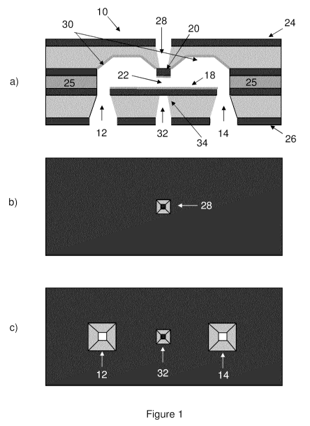
Figure 1 shows a schematic of a fluidic cell, including views of (a)
vertical section through a central plane of the cell, (b) the upper cell
surface,
and (c) the lower cell surface.
Figure 2 shows a schematic illustrating the fabrication steps of the
device.
Figure 3 shows an image of the membrane area of a nanofluidic cell,
in which fluorescence from within the cell is detected through the membrane.
The cell is empty in Figure 2(a) and filled with Rhodamine in Figure 2(b).
Figure 4 shows a holder used to clamp two halves of a nanofluidic cell
together, with drawings of (a) the upper and (b) lower pieces of the holder,
and an image (c) of the two pieces shown side by side.
Figure 5 shows the interference pattern obtained when imaging
through the membrane within a nanofluidic cell, in which the cell is (a)
evacuated, (b) partially filled with air, and (c) pumped with air.
Figure 6 provides a flow chart illustrating a method of actively
controlling the sample thickness during a measurement.
Figure 7 shows a schematic of a fluidic system in which a nanofluidic
cell is placed inside a vacuum chamber.
DETAILED DESCRIPTION OF THE INVENTION
Generally speaking, the systems described herein are directed to a
fluidic cell. As required, embodiments of the present invention are disclosed
herein. However, the disclosed embodiments are merely exemplary, and it
12
CA 02768873 2012-01-23
WO 2011/009209 PCT/CA2010/001139
should be understood that the invention may be embodied in many various
and alternative forms. The Figures are not to scale and some features may be
exaggerated or minimized to show details of particular elements while related
elements may have been eliminated to prevent obscuring novel aspects.
Furthermore, various aspects of the invention may be further reduced in scale
by using standard microfluidic concepts for flowing fluids involving
micropumps and valves as a replacement of the macroscale syringe pumps
shown in Figure 6. Therefore, specific structural and functional details
disclosed herein are not to be interpreted as limiting but merely as a basis
for
the claims and as a representative basis for teaching one skilled in the art
to
variously employ the present invention. For purposes of teaching and not
limitation, the illustrated embodiments are directed to nanofluidic cells.
As used herein, the terms, "comprises" and "comprising" are to be
construed as being inclusive and open ended, and not exclusive. Specifically,
when used in this specification including claims, the terms, "comprises" and
"comprising" and variations thereof mean the specified features, steps or
components are included. These terms are not to be interpreted to exclude
the presence of other features, steps or components.
As used herein, the terms "about" and "approximately", when used in
conjunction with ranges of dimensions of particles, compositions of mixtures
or other physical properties or characteristics, are meant to cover slight
variations that may exist in the upper and lower limits of the ranges of
dimensions so as to not exclude embodiments where on average most of the
13
CA 02768873 2012-01-23
WO 2011/009209 PCT/CA2010/001139
dimensions are satisfied but where statistically dimensions may exist outside
this region. It is not the intention to exclude embodiments such as these from
the present invention.
As used herein, the coordinating conjunction "and/or" is meant to be a
selection between a logical disjunction and a logical conjunction of the
adjacent words, phrases, or clauses. Specifically, the phrase "X and/or Y" is
meant to be interpreted as "one or both of X and Y" wherein X and Y are any
word, phrase, or clause.
A fluidic cell according to one embodiment is shown in cross-section in
Figure 1(a). The cell, shown generally at 10, includes an inlet port 12, and
outlet port 14, an internal flow path between the ports 12 and 14, and a
membrane 20. Membrane 20 and internal surface 18 located below the
membrane define the narrowest portion 22 of the flow path. As used herein,
the term "membrane" refers to a planar segment enclosing a portion of the
internal flow path, having a thickness selected to enable incident electrons,
acoustic waves, light, x-rays, and/or other forms of electromagnetic radiation
to enter the nanofluidic cell without experiencing significant attenuation,
thus
enabling the internal fluid to be probed. In non-limiting examples, the
membrane may comprise a locally thin portion of a substrate or may comprise
a portion of a layer deposited onto a substrate, where the membrane portion
of the layer comprises an internal surface enclosing a portion of the flow
path,
and an external surface exposed to the external environment.
14
CA 02768873 2012-01-23
WO 2011/009209 PCT/CA2010/001139
Fluid enters the cell through the inlet port, passes through a channel
between the membrane 20 and the internal surface 18, and exits through the
outlet port. All fluid entering the inlet port must pass through the channel
prior
to exiting through the outlet port. In the embodiment shown in Figure 1 (a),
the
channel is formed by the presence of a spacer layer 25.
Figures 1(b) and 1(c) show top and bottom views of the flow cell. The
cell includes an upper surface 24 and a lower surface 26, and further includes
a viewport 28 extending from the upper surface 24 to the outer surface of the
membrane 20. The inlet port 12 and outlet port 14 are located in the lower
surface 26. Viewport 28 is provided to expose the external surface of
membrane 20 to the external environment and recess the membrane from the
top surface 24 of the flow cell. As shown in Figure 1 (b), the membrane 20
extends in a direction perpendicular to the plane of the page in Figure 1(a)
to
produce a square planar structure. Alternate shapes and geometries may be
provided, such as a rectangular or circular planar shape. The cross-sectional
area of the membrane is selected based on the properties of the material
chosen and the application-specific window thickness.
In a preferred embodiment in which the membrane comprises silicon
nitride, the cross-sectional area is less than about 1 mm2, and the thickness
of the membrane is between 10 and 1000 nm. In embodiments in which the
membrane material comprises amorphous carbon or graphene, the
membrane thickness may be less than 10 nm. The preferred thickness of the
membrane depends on the nature of the beam used to probe the sample
CA 02768873 2012-01-23
WO 2011/009209 PCT/CA2010/001139
flowing through the nanofluidic cell. In the case of x-rays, a preferred
thickness range is from approximately 100 nm to 10 pm. In electron
microscopy applications, including electron holography, a preferred thickness
range is from approximately 10 to 100 nm. When the sample is probed via
optical radiation, a preferred thickness range is from approximately 10 nm to
pm. Thicker membranes allow a larger unsupported surface area, due to
the increased mechanical strength afforded by the material thickness.
The thickness of the narrow channel 22 formed between the
membrane and the internal surface is selected to enable the probing of the
10 sample under investigation, depending on the amount of absorption of the
incident probe beam by the sample. Specifically, the density and absorption
cross-section of the sample will dictate the preferred thickness of the
channel.
Furthermore, in applications in which it is desirable to include
characterization
where a primary probing beam causes emission of a secondary beam (e.g.
primary incident photons producing secondary electron emission), then the
sample and membrane must have a thickness that is selected to allow the
secondary beam to be emitted and be collected by the detector. Non-limiting
examples of secondary beams include optically generated beams such as
sum frequency generation and harmonic generation; acoustic waves such as
photo-acoustic generated waves, and secondary beams from scanning
electron microscopy including secondary and back-scattered electrons, x-
rays, and cathodoluminescence.
16
CA 02768873 2012-01-23
WO 2011/009209 PCT/CA2010/001139
The thickness of the narrow channel 22 may also be selected to allow
the passage of particles, cells or other species within the fluid. While a
preferred thickness range for the fluid flow defining the sample pathlength
includes approximately ten nanometers to approximately ten microns, thicker
or thinner pathlengths are also contemplated by embodiments of the
invention. The thickness of the channel giving rise to the sample path-length
is preferably controlled by the thickness of the spacer layer 25.
The thickness of the channel 22 also depends on whether the probe
beam will be detected in reflection mode or in transmission mode. In
reflection
mode, the signal obtained may be less sensitive to the thickness of the
channel. However, in transmission mode, the signal obtained is highly
sensitive to the thickness of the channel.
In an embodiment in which the cell is to be used in transmission mode,
the cell further includes a second viewport 32 extending from the lower
surface 26 to the outer surface of a second membrane 34. In this
embodiment, the minimum channel thickness 22 occurs between the first and
second membranes 20 and 34. As shown in Figure 1, the second membrane
may comprise a portion of internal surface 18 that extends in a transverse
plane spatially beyond the first membrane 20, or vice-versa, as the smaller
membrane defines the spatial extent of the channel. The second viewport 32
enables the transmission of the probe beam through the first membrane 20,
narrow channel 22, and second membrane 34, where it may be imaged,
17
CA 02768873 2012-01-23
WO 2011/009209 PCT/CA2010/001139
detected, or otherwise appropriately processed according to the desired
application.
In order to reduce fluidic resistance within the nanofluidic cell and
support the analysis of large fluid volumes in shortened time periods, the
flow
path outside of the narrow channel 22 has a cross-sectional area that
exceeds the cross-sectional area within the membrane region. An illustrative
embodiment is shown in Figure 1 (a), which is not to scale, where the cross-
sectional height in the vertical direction in the regions 30 on either side of
the
membrane region is shown as being larger than the thickness of the narrow
channel 22. Preferably, the cross-sectional dimensions in at least a portion
of
the non-membrane region are greater than approximately 10 microns.
In the specific embodiment shown in Figure 1 (a), trenches 30 are
provided on either side of the narrow channel 22, producing an increased
cross-sectional area orthogonal to the flow direction that tapers in size
towards the channel. This design and similar designs with a narrow channel
but otherwise broad flow path allow fluid to pass through the cell with
minimal
fluidic resistance. Accordingly, the flow channels of the present device have
dimensions such that the probed region is filled whenever flow is achieved
between the two access ports of the device. In addition, the high flow-
resistance region is preferably limited to the narrow channel 22 to reduce
fluidic resistance, resulting in rapid filling rates and an improved response
to
external pressure. Both features can be beneficial when actively controlling
18
CA 02768873 2012-01-23
WO 2011/009209 PCT/CA2010/001139
the flow of sample through the cell using an external pump, as further
described in additional embodiments below.
In a preferred embodiment, the fluidic resistance within the flow cell is
sufficiently low such that the time response of membrane deformations to
pressure changes occurs on timescales from approximately 1 ms to 10 sec to
support active feedback stabilization of the channel thickness. Active
stabilization of the channel thickness is of significant importance when the
membrane has a thickness on the nanometer to micron scale, and is prone to
mechanical deformation.
In methods known in the prior art, to this invention, it was not possible
to flow fluids, gases or liquids, without causing either mechanical
instabilities
in the path length or rupture of the membrane or a lack of confinement of the
liquid to the flow channels. However, in transmission-based imaging and
spectroscopic methods, one requires stable sample thicknesses so as to not
obscure or blur the observable. The embodiments disclosed herein thus
provide a flow cell having dimensions that reduce resistance to fluid flow so
as to decrease the response time of membrane deformations and associated
path-length variations, thereby permitting active feedback stabilization of
the
fluid flow. This approach can be employed to achieve stable flow with sample
path-lengths variable from the nanometer to micron scale with path-length
stabilization of nanometer precision as required for the stated applications.
More preferably, the active control mechanism is adapted to control the
height of the channel 22 with precision on a nanometer length scale.
19
CA 02768873 2012-01-23
WO 2011/009209 PCT/CA2010/001139
Laterally, the preferred distance between the access ports of the device is on
the order of 1 cm. Such a macroscopic distance is preferred to allow
sufficient
space for O-rings or other sealing devices or means that interface the ports
with a device holder (discussed in further detail below) and to have a view
port in the center of the device through which the sample is probed. As noted
above, driving fluids over centimeter distances within a channel having a
cross-sectional height that is very small, for example, in the nanometer or
micron range, is problematic due to the extremely low flow rates. For
instance, calculations show that the time it takes for water to cross a 1 cm
length channel, with 100 nm cross-section is approximately 5 minutes. A slow
filling time implies a slow response time to changes in external pressure. A
fast response time is desirable for actively controlling the bowing of the
viewports using the transmitted (or reflected) signal as feedback (as
discussed further below).
Therefore, as shown in Figure 1, trenches which widen the cross-
sectional length of the flow region adjacent to the narrow channel 22 are
included for achieving fast flow rates. In a preferred embodiment, the
trenches have a thickness on a micron scale, and more preferably have a
thickness of at least 10 microns. The narrow channel 22 in the membrane
region, where high flow-resistance occurs, is preferably on the nanometer to
micron scale. Preferably, the channel has a minimum thickness less than
approximately 1 micron, and more preferably less than about 100 nm. The
minimum thickness preferably occurs over a transverse length that is less
CA 02768873 2012-01-23
WO 2011/009209 PCT/CA2010/001139
than approximately 1 mm, and more preferably less than about 500 m. In a
preferred embodiment, this results in <1 sec filling time of the cell. In a
preferred embodiment, one or more internal surfaces forming the internal flow
path may be coated with a material that modifies the surface properties of the
internal flow path, such as the surface tension, hydrophobicity or
hydrophilicity to increase surface adhesion and assist flow through capillary
forces as appropriate for the fluid of interest. Alternatively, chemical
agents
may be added to the fluid to change its surface tension.
Although Figure 1(a) shows the second membrane 34 as having
approximately the same size (i.e. freestanding spatial extent) as the first
membrane, various embodiments may be practiced with different sized
membranes. Furthermore, while the internal surface 18 extends spatially
beyond the second membrane 34, it is also possible for the internal surface
18 to be formed essentially membrane 34, as in the case of the first
membrane 20. Accordingly, trenches such as those shown in Figure 1 may
also be provided adjacent to the second membrane 34, thereby limiting the
spatial extent of the internal surface 18.
In another embodiment, the inlet and outlet ports may be provided in
the upper surface of the cell instead of the lower surface, or alternatively
laterally in the sides of the cell. Alternatively, the inlet and outlet ports
may be
provided on opposite sides of the cell.
In a preferred embodiment, the nanofluidic cell is fabricated on two
separate substrates that are joined (e.g. clamped or bonded together).
21
CA 02768873 2012-01-23
WO 2011/009209 PCT/CA2010/001139
Suitable clamping or bonding means include but are not limited to mechanical
clamping, adhesives, ultrasonic welding, thermal annealing, anodic bonding,
and silicon fusion bonding. In another embodiment, the nanofluidic cell
comprises two substrates that are identically processed and subsequently
joined to form a cell according to the aforementioned embodiments.
Secondary inlet or outlet ports may be used to add additional fluid or
supplementary buffers or reagents, or to provide an additional means to
control the pressure within the cell. Alternatively, the ports may be provided
in
the side of the cell, or opposite upper and lower surfaces of the cell, in
which
case the two substrates may be joined to provide a single inlet port and a
single outlet port.
While the cell may be fabricated from a single type of material, a
preferred embodiment includes separate layers for the membrane. The layers
may be formed by coating a surface of the substrates and subsequently
processing the coated layer to remove most of the layer, leaving only the
small planar region forming the membrane. More preferably, a spacer layer
formed from a third material is included for defining and assisting in
maintaining the thickness of the channel outside of the membrane region.
In a preferred embodiment, the substrates are formed from silicon
20 wafers, although other wafer materials known in the art, such as wafers
comprising other semiconductor materials, may be employed. In an
embodiment in which the substrates are silicon, the membrane is preferably
formed from silicon nitride. In another preferred embodiment, the membrane
22
CA 02768873 2012-01-23
WO 2011/009209 PCT/CA2010/001139
is boron nitride. In other embodiments, the membrane may be formed from
silicon carbide, graphene, carbon films, diamond and other allotropes of
carbon, molybdenum disulphide, silicon and silicon dioxide. The spacer layer
may formed from a layer of silicon dioxide, polycrystalline or amorphous Si,
photoresist, Teflon TM spacers, titanium spacers, and other spacer materials
known in the art.
In applications involving electron microscopy, the membrane is
preferably a SiN membrane with a thickness of approximately 50 nm, which is
a suitable thickness for use as a view port. The surface area of the view
ports
is preferably approximately 50x50 um2, sufficient for the electron beam in a
TEM to pass through. A preferred minimum channel thickness as defined by
spacer layer (preferably Si02) is about 100 nm.
A nanofluidic cell according to embodiments described herein may be
formed using a variety of known materials processing methods, including, but
not limited to, chemical vapor deposition, lithography, chemical etching,
micromachining, laser micromachining, and embossing, or any combination
thereof. In a preferred embodiment, chemical vapor deposition, lithography
and chemical etching are used to achieve the desired microstructure. In
addition, implementations that require a thicker (for example, greater than 10
um) channel may employ a machined Teflon or silicone spacer to define the
sample length.
The following example provides a preferred embodiment of the
nanofluidic cell and a method for forming the nanofluidic cell. In a preferred
23
CA 02768873 2012-01-23
WO 2011/009209 PCT/CA2010/001139
embodiment, the cell is formed from two substantially planar substrates with
channels formed therein that are pressed or clamped together to form the
internal flow path, where the one or both of the substrates includes a thin
layer forming the membrane. Preferably, the substrates are silicon and the
membrane is low stress silicon nitride, which can be back-etched to form the
membrane on one or both of the silicon substrates using potassium hydroxide
(KOH). The thickness of each of the silicon nitride membranes is preferably
less than 50 nm. With reference to Figure 1, the minimum channel thickness
between the silicon nitride membranes may be defined by a spacer 25,
preferably comprising silicon oxide, that is deposited on one or both
substrates before the matching pieces of the structure are clamped or bonded
together. The narrow channel 22 may then be formed by etching the silicon
oxide spacer layer using buffered oxide etch (BOE). The depth of the narrow
channel 22 is defined by the thickness of the deposited silicon oxide layer.
This is chosen based on the characteristics of the sample under investigation,
for example, the density and the electron (or X ray) scattering cross-section
or
the optical absorption, and can preferably range from a few tens of
nanometers to a few microns. In experiments where macroscopic sample
lengths are desired (such experiments involving hard X rays, where sample
thicknesses can be 10-100 m), the silicon oxide spacer may be replaced by
another spacer made from a material capable of forming a fluidic seal, such
as TeflonTM. For hydrophilic liquids, a 5 nm coating layer of silicon oxide
may
24
CA 02768873 2012-01-23
WO 2011/009209 PCT/CA2010/001139
be applied in order to enhance the flow rate, or chemical agents may be
added to the fluid to change its surface tension.
Figure 2 illustrates the fabrication steps of a nanofluidic cell according
to a preferred embodiment. It is to be understood that the fabrication steps
described below provide a non-limiting example and that a nanofluidic cell
according to embodiments disclosed above may be fabricated by a variety of
other methods. Starting with a pair of Si substrates 50 (Figure 2(a)), a low
pressure chemical vapor deposition chamber is used to deposit a layer of low
stress silicon nitride 52 on both sides of each substrate (Figure 2(b)). A
combination of photolithography and reactive ion etching is used to create the
window pattern 54 in the top substrate, and the window pattern 56 plus the
two access holes patterns 58 in the bottom substrate (Figure 2(c)). KOH is
used to etch the exposed window pattern in the top substrate from the top
surface to the silicon nitride layer, resulting in a free-standing membrane
60,
and the exposed features 62 on the bottom substrate are etched partially
(preferably about half-way) through the bulk of the Si substrate (Figure
2(d)).
A combination of photolithography and reactive ion etching is used to create
the two trench patterns 64 in the bottom substrate (Figure 2(e)). This process
involves backside alignment of the photolithographic mask with the already
etched KOH features during the previous step. The bottom substrate is
inserted again into KOH so that etching proceeds from both sides of the
substrate, thus joining the access holes 58 with the trenches 64 (Figure
2(f)).
To form the spacer layer, a layer of silicon oxide 66 is deposited on one side
CA 02768873 2012-01-23
WO 2011/009209 PCT/CA2010/001139
of the top substrate using plasma enhanced chemical vapor deposition
(Figure 2 (g)). Alternatively, a layer of polycrystalline silicon may be
deposited and subsequently oxidized to form the spacer layer. A combination
of photolithography and buffered oxide etching is used to define the channel
pattern 68 in the top substrate (Figure 2(h)) (note that in this example, the
steps shown in Figure 2(g) and 2(h) may be executed any time after the step
shown in Figure 2(d). In an optional step, the hydrophilicity of the finished
surfaces may be enhanced by depositing a layer of silicon oxide 70
(preferably approximately 5 nm) using plasma enhanced chemical vapor
deposition (Figure 2 (i)). Alternatively, if a nonpolar solvent is employed,
the
surfaces may be made hydrophobic. Once clamped or bonded together, the
fabricated structure forms an enclosure bounded by two silicon nitride
windows and accessible to the outside world through a system of channels
(Figure 2 (j)).
While the above example describes a method of fabricating a
nanofluidic cell in which the inlet and outlet ports are located in the lower
substrate forming the cell, and the trenches are also provided in the lower
substrate the cell, it will be readily apparent to those skilled in the art
that
other orientations of the inlet and outlet ports and the trenches are
possible.
For example, the inlet and outlet ports can be provided in the upper
substrate,
or alternatively one port may be located in the upper substrate and another
port can be located in the lower substrate. Also, the trenches can be located
26
CA 02768873 2012-01-23
WO 2011/009209 PCT/CA2010/001139
in the upper substrate, as illustrated in Figure 1. As noted above, in an
alternative embodiment, the ports may be formed in the side of the cell.
The fabrication steps described in Figure 2 represent one embodiment
in which the trenches and access ports are created in the bottom substrate
while the spacer is created in the top substrate. In general there is no
preference with respect to which substrate (top or bottom) each of these 3
features (trenches, access ports, and spacer) should be created in. For
instance, in an alternative embodiment all 3 features are created in the same
substrate, while the second substrate contained only a view port. In this
case,
the fabrication of the spacer should be done as the final step because the
other two features require KOH etching, which is destructive to the Si02
spacer.
Optical microscope images of the sample area of a nanofluidic cell
fabricated according to the steps described in Figure 2 are shown in Figure 3.
Figure 3(a) is an image of an empty cell under taken under illumination in the
450-490 nm. Figure 3(b) is a picture of a cell filled with Rhodamine dye in
solution to clearly demonstrate the liquid filled the nanofluidic cell.
A stainless steel sample holder was designed to clamp together the
matching pieces of the nanofluidic cell. Figures 4(a) and 4(b) show the upper
100 and lower 150 pieces of the holder, respectively, and Figure 4(c) shows a
photograph of the two disassembled pieces of the sample holder. The
nanofluidic cell is clamped between the two pieces of the holder, and the
27
CA 02768873 2012-01-23
WO 2011/009209 PCT/CA2010/001139
holder allows sample delivery to the cell chamber through a system of
embedded channels.
The top piece of the holder includes four holes 102 for inserting
fasteners (not shown) that are received in threaded holes 152 in the bottom
piece of the holder. Also included in the top piece are four holes 104 for
supporting guide pins (not shown) that are received in adjacent holes 154 in
the bottom piece. The incident beam for illuminating the sample is directed
through a central via 110 in the top piece that terminates in a cylindrical
opening 115. Similar features are provided in the bottom piece at 160 and
165, respectively to enable the detection of the beam transmitted through the
sample. An o-ring (shown in the image) is included in each cylindrical opening
to protect against fluid leakage in the event of the rupture or breakage of
the
membrane.
The cell is aligned between the holders so that the inlet port 12 and
outlet port 14 are positioned directly above the central opening in the two
lateral cylindrical openings 170 and 171 in the bottom piece. The lateral
cylindrical openings are connected to channels that include a right angle,
thus
enabling the fluid to be pumped into and out of the holder in the horizontal
plane. The channels connect on one end to the inlet and outlet ports of the
cell and seal via o-rings, and on the other end to flat-bottom ports that are
used to fasten 1/16" tubing to the holder using standard fluidic fittings. As
shown in Figure 4(b), the channel can be narrowed prior to connecting with
the cylindrical openings 170 and 171 to limit the volume of sample. The inner
28
CA 02768873 2012-01-23
WO 2011/009209 PCT/CA2010/001139
region of the holder is further optionally protected from leaks by the
incorporation of an outer o-ring, which is shown in the image and is housed in
the circular indentation 158.
A common problem in dealing with a nanoscale thin membrane is that
the flexibility of the membrane causes it to bow due to both the residual
stress
from the deposition process, and the difference in pressure between the cell
chamber and the outside environment. Bowing may result in a sample
thickness that greatly exceeds the gap as defined by the silicon oxide spacer.
This effect is demonstrated in Figure 5, where the sample chamber was
optically imaged under different pressure conditions. In Figure 5(a), the
sample chamber is evacuated, leading to the collapse of the two silicon
nitride
membranes. In Figure 5(b), the sample is partially filled with air. In Figure
5(c), the sample chamber is completely pumped with air. The interference
fringes indicate variation in the cell thickness over the membrane area.
The problem may be addressed by actively controlling the pressure
inside the cell chamber using a computer-controlled pump and feedback from
measurements made in the cell. As shown in the flow chart provided in
Figure 6, a signal, such as transmission through the cell may be monitored in
step 200. A computer or processor is employed in step 210 to process the
measured signal, where a pre-determined relationship between the measured
signal and the channel thickness is employed to infer a deviation of the
channel thickness from a preferred value. In step 220, a feedback signal is
provided to the fluid handling apparatus for maintaining a controlled sample
29
CA 02768873 2012-01-23
WO 2011/009209 PCT/CA2010/001139
thickness throughout the period over which a measurement or experiment is
carried out. This process may be repeated to actively stabilize the flow cell.
As noted in aforementioned embodiments, the trenches, which limit the high
resistance-flow region to the sample area, play an important role in the
active
control mechanism since they essentially reduce the response time of the
system to changes in pumping pressure. A responsive system, in turn, allows
the feedback error to converge quickly. This system also explicitly exploits
the high damping of fluids over this timescale to produce a stable flow
pattern
through the cell.
The aforementioned method in which the total transmitted or reflected
field, intensity or power is monitored to stabilize the geometry of the cell
is
best suited for applications in which the fluid flowing through the cell is
homogeneous. In fluids with heterogeneity, variations in absorption may
preclude the use of total field, intensity or power alone. Accordingly, a
preferred embodiment involves analyzing the signal transmitted or
backscattered from the cell and adjusting the applied cell pressure to keep
some metric pertaining to the signal within the desired range. In optical
spectroscopy, a useful metric could be the total transmitted power of the
probing beam, while in electron microscopy it could be the total integrated
intensity of the detected image. In a particular embodiment involving the
generation of X-rays within a sample in a fluidic cell, the sample thickness
may be controlled by a feedback method. X-ray generation from electrons
interacting with the sample and sample cell are dependent upon several
CA 02768873 2012-01-23
WO 2011/009209 PCT/CA2010/001139
factors that can include the incident electron energy, the atomic composition
of the cell windows and sample, and the thickness of the windows and
sample. For a given sample, sample cell and fixed electron energy, actively
changing the thickness of the sample by adjusting the fluid pressure will
result
in a change in the x-ray yield. Accordingly, in a preferred embodiment, the x-
ray yield can be fed back to the pump in order to control the sample thickness
in the cell through flexing of the membrane, as outlined in the previous
feedback schemes.
In another embodiment involving an active feedback method, the
sample thickness may be controlled via electron beam attenuation. An
electron beam of fixed electron energy transmitting through a given substance
inside a nanofluidic cell with fixed window thicknesses will be attenuated to
a
degree depending on the thickness of the sample. By monitoring the
magnitude of the transmitted electron flux through the sample, for example,
through the diminished signal from a phosphorescent screen or CCD detector
or imaging plate or other readout device such as a microchannel-plate anode
readout, one can use the degree of signal attenuation to directly monitor the
thickness of the sample.
When using the electron beam in diffraction mode, a preferred method
includes monitoring the intensity of the central s=0 (s is the scattering
vector)
spot using the method outlined above, or even a Faraday cup, for instance.
The intensity of the central, s=0, spot will diminish with increasing sample
thickness. In diffraction mode, an alternative embodiment involves monitoring
31
CA 02768873 2012-01-23
WO 2011/009209 PCT/CA2010/001139
the intensity of Bragg peaks or Debye-Scherrer rings in order to obtain a
signal dependent on the sample thickness. With increasing sample thickness
(fixed window thicknesses and for a given sample), the intensity distribution
of
the peaks (or rings) will change owing to sample-thickness-dependent
multiple scattering. In a preferred embodiment, one may also stabilize the
sample thickness by selecting a given intensity (chosen based on a criterion
by which multiple scattering is minimized) and feedback the pump pressure to
minimize the change in the intensity.
In another preferred embodiment, the sample thickness may be
actively controlled by monitoring the diffraction pattern. When the
nanofluidic
cell window material gives a crystalline diffraction pattern (well-separated
Bragg peaks), or polycrystalline diffraction pattern (Debye-Scherrer ring) or
possibly even an amorphous ring, the scattering vectors at which those peaks
or rings occur is a function of the unit cell dimensions. When the windows are
bowed owing to an increase in sample pumping pressure that increases the
sample thickness, then the macroscopic deflection of the windows may be
detectable as a change in the diffraction-pattern-derived unit cell
parameters.
Changes in the diffraction pattern would indicate changes in the degree of
deflection of the nanofluidic cell membranes, which in turn would indicate a
change in the effective sample thickness. Therefore, in a preferred
embodiment, the scattering vector magnitude for given diffraction pattern
peaks/rings is used to feed back to the pump driving the sample in order to
control the sample thickness. One skilled in the art will readily appreciate
that
32
CA 02768873 2012-01-23
WO 2011/009209 PCT/CA2010/001139
this feedback method is dependent on being able to distinguish the diffraction
pattern (or amorphous ring) of the nanofluidic cell windows from that of the
sample.
To facilitate flow for such active feedback stabilization, the design
implements a single channel that is wide enough to overlap with the area in
between the silicon nitride membranes. Preferably, access holes which
deliver the fluid to the cell chamber are connected to the channels imbedded
in the sample holder through o-rings. Accordingly, the fluid has a single path
to traverse from one inlet to the other. This feature is important for two
reasons. First, it insures that the cell chamber is filled. Second, it allows
efficient control of flow of sample in the cell chamber. In contrast, designs
which rely on two silicon nitride windows without a channel system may flood
the whole area outside the cell structure with the sample. In such devices,
the fluid can potentially bypass the cell chamber once it faces resistance and
instead go around the membrane region. This leads to an empty or partially
filled cell that is unresponsive to applied pressure, therefore, offering no
control over the sample thickness.
Figure 7 shows a system including a nanofluidic cell system 300
according to the aforementioned embodiments. The system includes a
nanofluidic cell housed in a holder 310, tubing 320 connecting the cell to a
pump 330 and an output reservoir or a second pump (not shown). In a
preferred embodiment, the pumps (i.e. sample delivery means) are syringe
pumps 340. Actuation of the pump causes fluid (e.g. sample) to flow through
33
CA 02768873 2012-01-23
WO 2011/009209 PCT/CA2010/001139
the cell, where it can be investigated by directing a probe beam through the
membrane surface. In a preferred embodiment, the pump system may be
reduced in size by using microfluidic pumps and valves for the input and
output feeds.
In a preferred embodiment, the system is employed in an electron
microscope and the nanofluidic cell is located inside a vacuum chamber.
Tubing and connection means such as ports and fittings 350 housed in the
vacuum chamber wall 360 (or other fittings known in the art) are employed to
connect tubing within the vacuum chamber to tubing under ambient
conditions.
As will be appreciated by those skilled in the art, the nanofluidic cell
disclosed herein can be adapted to a wide range of configurations and
applications. Preferably, the nanofluidic cell is included within an electron
microscope system, enabling the direct imaging and analysis of fluids
(comprising liquids and gases), or the imaging of solids contained within
fluids
with an electron microscope. In a preferred embodiment, a system is provided
for the analysis of various biological species in their natural fluidic
environments, including, but not limited to, nucleic acids, proteins, and
macromolecular assemblages such as cells.
While preferred embodiments of the cell are adapted for transmission
and reflection measurements, other signal detection means may also be
employed. For example, species inside a fluid flowing through the cell may be
excited optically or with other means, such as an electron beam, and the
34
CA 02768873 2012-01-23
WO 2011/009209 PCT/CA2010/001139
emission of photons, acoustic waves or electrons may be detected.
Exemplary applications include fluorescence, time-resolved fluorescence,
luminescence, Raman scattering, surface-enhanced Raman scattering, X-ray
diffraction, electron energy loss spectroscopy, photo-acoustic spectroscopy,
and energy-dispersive X-ray spectroscopy.
In another embodiment, a system is provided for performing
microscopy and analysis on biological fluids containing cells and other
structures. For example, in one embodiment, the nanofluidic cell provides an
improved cell for use in a flow-cytometer or particle analysis system. In
particular, flowing biological cells through a nanofluidic cell enables
electron
microscope flow cytometry, which can be adapted for a wide range of
research and clinical uses. The system can also be used for the imaging and
analysis of nanoparticles in a fluidic or biological environment.
While the aforementioned embodiments have disclosed the use of
liquid samples, or liquid samples containing biological media such as cells,
the sample may alternatively comprise a gas.
Due to the fluidic nature of the nanofluidic cell system, additional
embodiments contemplate uses and applications involving separation
methods. For example, by coupling a separation means such as liquid
chromatography or electrophoresis to the system, a novel analysis system is
provided in which chemical, structural or molecular species in a fluid are
first
spatially separated and subsequently analyzed serially in the nanofluidic
cell.
CA 02768873 2012-01-23
WO 2011/009209 PCT/CA2010/001139
The foregoing description of the preferred embodiments of the
invention has been presented to illustrate the principles of the invention and
not to limit the invention to the particular embodiment illustrated. It is
intended
that the scope of the invention be defined by all of the embodiments
encompassed within the following claims and their equivalents.
36