Note : Les descriptions sont présentées dans la langue officielle dans laquelle elles ont été soumises.
CA 02825329 2013-07-22
METHOD AND DEVICE FOR REALIZING SPECIFIC ABSORPTION RATE
(SAR) CONTROL
TECHNICAL FIELD
The disclosure relates to the communication field and in particular to a
method and
device for realizing Specific Absorption Rate (SAR) control.
BACKGROUND
With the rapid development of wireless communication technology, wireless
terminals (mobile phone, data card, MiFi/Hotspot product) have been applied
more and
more widely. At the same time, the influence of electromagnetic radiation on
human
bodies brought about by the wireless terminal has become a public concern.
Most existing SAR reducing techniques adopt a method such as reduction of
transmitter power, use of wave absorbing material or of a conductor reflector
and shield,
and radiation-proof and wave-absorbing coating on a casing surface, etc.,
which will not
only increase costs and process complexity, but also affect a communication
signal,
thereby failing to fundamentally solve the contradiction between human body
radiation
safety and high-quality wireless communication. In addition, more space is
required for
the location of the reflector and shield during assembly, which is contrary to
the purpose
of miniaturized design of the wireless terminal.
Additionally, a mechanism of forming a local SAR peak value is the joint
contribution
from the surface current of an antenna conductor per se and the surface
current induced
on metal surfaces in the antenna near field, such as a Printed Circuit Board
(PCB) metal
ground, a shielding cover, and a shielding frame. In a wireless terminal
device, the
exposed circuit shielding cover, PCB substrate metal ground, housing, and the
antenna
would interact with each other to form a complicated boundary condition. The
SAR peak
value generally appears near a maximum local current at the antenna or a PCB
metal
surface. Currently, the parasitic conductor structures such as a PCB grooving
or a
conductive ring structure are usually added near the antenna or on the PCB to
alter the
surface current distribution, so as to reduce an SAR value. However, such
technique
takes up much more space, and is applicable to one-directional SAR reduction
for a
product such as the mobile phone, but not applicable to a data card wireless
terminal
product.
2
= CA 02825329 2013-07-22
SUMMARY
In view of this, the main objective of the disclosure is to provide a method
and
device for realizing SAR control, so as to reduce the local SAR peak value and
lessen
the harm of radiation to human bodies.
To achieve this objective, the technical solution of the disclosure is
realized as
follows.
A method for realizing Specific Absorption Rate (SAR) control, includes:
providing phase shifters on the metal ground edge of a wireless terminal; and
altering an induced current of the metal ground edge by applying the phase
shifters,
such that an antenna near field radiation characteristic of an SAR can be
reduced.
The providing phase shifters may be:
introducing the phase shifters consisting of a plurality of lumped circuit
elements on
the PCB metal ground edge of the wireless terminal.
The altering an induced current of the metal ground edge may be:
altering an induced current distribution on a PCB of the wireless terminal by
altering
magnitudes of phase shift and locations of the phase shifters on a metal
ground.
Altering the antenna near field radiation characteristic may be:
altering phases and amplitudes of current elements on the metal ground edge by
applying the phase shifters, so that these current elements produce a reversed-
phase
superposition during near-field radiation to reduce the value of the SAR.
The method may further include:
performing real-time monitoring of a phase and amplitude of the induced
current on
the metal ground edge through electronic tuning control, and adjusting phase
shift values
of the phase shifters correspondingly to realize dynamical/real¨time
adjustment of an
SAR value.
A device for realizing Specific Absorption Rate (SAR) control, includes a
structure of
a wireless terminal, wherein phase shifters are provided on the metal ground
edge of the
device, the phase shifters being configured to alter an induced current of the
metal
ground edge such that an antenna near field radiation characteristic of an SAR
can be
reduced.
3
CA 02825329 2013-07-22
The phase shifters may be realized through a passive lumped element or an
active
element;
the passive lumped element may include one of a Resistor-Capacitor (RC) phase
shifting network, an inductor-Capacitor (LC) phase shifting network, a diode
phase
shifter, and a ferrite phase shifter; and
the active element may include one of an operational amplifier, a switch, a
variable
capacitance diode, and a reversible dual-mode ferrite phase shifter.
The phase shifters may be provided on the PCB metal ground edge of the
wireless
terminal, on specific locations determined by an induced current distribution,
in surface
induced current accumulation areas.
A PCB metal edge area and a PCB central area in the device may be divided
through slotting, and the phase shifters may bridge both sides of a slot
formed by the
slotting; or
a ground plane of an interlayer of a multi-layer PCB may be used as a
reference
ground (GND), and a circuit network of the phase shifters may be connected
through an
inter-layer through hole structure.
The phase shifters may be further configured to perform real-time monitoring
of a
phase and amplitude of the induced current on the PCB metal ground edge and
adjust
phase shift values correspondingly to realize dynamical/real¨time adjustment
of an SAR
value
The method and device of the disclosure can alter current phase and amplitude
distribution of the metal ground without affecting the reception and
transmission
performance of the terminal, so as to reduce a local SAR peak value and lessen
the
harm of radiation to human bodies. Furthermore, the disclosure does not
require any
major change in a structure, circuit, and, antenna of a designed model, and
can save
space. The disclosure bears great flexibility and adaptability in an
application, thereby
realizing the objective of miniaturized design of the wireless terminal.
BRIEF DESCRIPTION OF THE DRAWINGS
Fig. 1 is the diagram of the two-dimensional structure of a common wireless
terminal
data card;
Fig. 2 is the schematic diagram of equivalent operation of a monopole antenna
on a
4
CA 02825329 2013-07-22
wireless terminal;
Fig. 3 is the schematic diagram of the two-dimensional structure of a low-SAR
data
card with a plurality of phase shifters;
Fig. 4a and Fig. 4b are schematic diagrams of circuit forms of an LC phase
shifting
network and an RC phase shifting network;
Fig. 5a and Fig. 5b are schematic diagrams of two ways of loading phase
shifters on
a PCB metal ground edge; and
Fig. 6 is the flowchart for realizing SAR control according to an embodiment
of the
disclosure.
DETAILED DESCRIPTION
Generally speaking, in order to reduce a SAR value without affecting the
overall
radiation quality of an antenna of a wireless terminal, phase shifters
consisting of a
plurality of lumped circuit elements may be introduced on a PCB metal ground
edge of a
data card to alter an antenna near field radiation characteristic by altering
a phase and
distribution of an induced current of the PCB metal ground edge, thereby
achieving the
objective of reducing the SAR value.
To achieve this objective, the technical solution of the disclosure is
realized as
follows:
specifically, the wireless terminal may include: a single-layer/multi-layer
PCB with
a radio frequency baseband circuit, a main antenna for transmission and
reception, a
diversity/MIMO antenna for reception, a structure housing, a USB connector,
and a
plurality of phase shifters located on the PCB metal ground edge. As the
plurality of
phase shifters are added on the PCB metal ground edge of the wireless
terminal,
therefore by altering phases and amplitudes of current elements on the metal
ground
edge, these current elements may produce a reversed-phase superposition during
near-field radiation, thereby reducing a local field strength peak value.
Specifically, an
induced current distribution on the PCB may be altered by altering magnitudes
of phase
shift and amplitude shift as well as locations of the phase shifters on a
medal ground.
The phase shifters may be realized through a passive lumped element, such as
one of a
Resistor-Capacitor (RC) phase shifting network, an inductor-Capacitor (LC)
phase
shifting network, a diode phase shifter, and a ferrite phase shifter, etc.; or
may also be
realized through an active element, such as one of an operational amplifier, a
switch, a
5
CA 02825329 2013-07-22
variable capacitance diode, and a reversible dual-mode ferrite phase shifter,
etc.
Further, real-time monitoring of a phase and amplitude of the induced current
on the
PCB metal ground edge may be performed through electronic tuning control, and
a
phase shift value of each phase shifter may be adjusted correspondingly, so as
to realize
a function of dynamical/real¨time adjustment of an SAR value.
According to the antenna theory, an antenna near-field is determined by the
radiation superposition of each sub-current source or element, and an electric
field local
extreme value may be formed in the case of phase coincidence. At the same
time, a
transmitting antenna induces a current on a surface of the PCB, wherein the
current
usually accumulates around the metal ground edge. Therefore, additional phase
shift
may be introduced to a surface current in a relatively small physical space
via
lumped-element phase shifters, causing phase cancellation of each sub-current
source
or element or increasing random perturbation of the surface current, so that
near-field
radiation is distributed as uniformly as possible, thus reducing an SAR
hotspot peak
value. At the same time, the phase shifters do not notably weaken an antenna
far-field
radiation characteristic of the data card, thus ensuring the quality of a
communication
signal.
In addition, as the phase shifters are only added on the PCB metal ground
edge, not
much physical space is required, and there is much flexibility and
adaptability in
application, which facilitates miniaturized design of the wireless terminal.
In a practical application, a current mainstream data card type wireless
terminal
device mostly adopts the form of a cube, and is connected to a laptop through
a USB
connector at an end. Meanwhile, a multi-mode data card (WCDMA, CDMA2000, and
LTE etc.) generally adopts a dual-antenna structure: the main antenna is
responsible for
transmission and reception, and an auxiliary antenna (MIMO antenna) is
responsible for
reception. The quality of the received signal and transmission throughput can
be
improved effectively through dual-path reception. Fig. 1 is a two-dimensional
view of a
dual-antenna data card terminal, wherein an end of a data card housing 1 is
provided
with a USB connector 2. The data card housing 1 further includes a PCB 3
provided with
a circuit element, a metal ground, and a shielding cover 6. A main antenna
area 4 is
located at the top of the data card, and an auxiliary antenna area 5 is
usually located on
a side of the data card. As required by miniaturization of a data card type
terminal
product, the main antenna is usually designed into the form of a monopole 7,
while the
6
CA 02825329 2013-07-22
PCB 3 functions as a ground of the monopole antenna. When the main antenna
operates, the metal ground of the PCB 3 is involved in the radiation, and
serves as
another part of antenna radiation.
Fig. 2 is a diagram of the equivalent operation principle of a small antenna
of the
monopole type. A feed source 8 feeds monopole antenna 7 and the metal ground
of PCB
3. The whole data card radiation unit may be equivalent to a dipole antenna
with an
unbalanced structure. Relatively large unbalanced induced currents exist on
the metal
ground of PCB 3 due to the existence of the unbalanced structure. Secondary
radiation
of these induced currents and radiation of the current on monopole antenna 7
have
phase superposition in the near field, forming local accumulation of
electromagnetic
energy. Generally, all monopole-type terminal small antenna have relatively
high SAR
values.
In order to reduce an SAR value, perturbation may be performed to induced
currents on PCB 3 to intervene in the phase superposition of near field
radiation.
Specifically, the plurality of phase shifters may be added to the metal ground
edge of the
PCB to alter the phase and amplitude distribution of a sub-current source or
element of
the metal ground edge. Fig. 3 is an application example of a low-SAR data
card, wherein
a radio frequency feeder 6 is connected to a radio frequency power amplifier
output
terminal and a main antenna feeding point. The feeder 9 usually has a
relatively large
surface current, and is not connected to the metal ground of PCB 3. Main
antenna area 4
includes clearance area 10 on the PCB, configured to ensure the radiation
performance
of the monopole antenna. A plurality of phase shifting units 11 are placed on
the metal
ground edge of PCB 3 and are configured to provide additional phase and
amplitude
bias for an accumulated current. The phase of various sub-current elements
cancels,
thus reducing a near field SAR hotspot peak value. Locations of the phase
shifting units
are determined by the induced current distribution, and the phase shifting
units should be
placed in surface induced current accumulation areas in principle, e.g. on the
PCB metal
ground edge and near the area of the feeder 9.
Additionally, the phase shifters may be realized in various forms. Fig. 4
illustrates
two simple passive lumped element phase shifter circuits, wherein Fig. 4a is
an LC
phase shifting network while Fig. 4b is an RC phase shifting network. The
specific rated
value of each element is calculated from a required phase shift amount and an
operating
frequency. It should be noted that both circuit networks need a unified
reference ground
7
CA 02825329 2013-07-22
(GND) plane.
In view of the requirement of a circuit network in Fig. 3 on the GND, Fig. 4
provides
two realization solutions for loading the phase shifters on the PCB metal
ground edge.
According to a current edge effect and proximity effect, a high-frequency
surface current
usually accumulates in the edge portion of the PCB metal ground, while a
current in the
central area of the metal ground is relatively small. Therefore, with respect
to the edge,
the central area of the metal ground may serve equivalently as the GND of a
high-frequency signal. Slotting is adopted as shown in the figures; An
elongated through
slot 12 as shown in Fig. 5a and local slots 13 as shown in Fig. 5b are adopted
to divide a
PCB metal edge area and a PCB central area. The phase shifters bridge both
sides of
the elongated through slot 12 or of a local slot 13, and may realize layout
and wiring of
the RC or LC circuit network. Another feasible solution is that the ground
plane of an
interlayer of the multi-layer PCB is taken as the GND, and connection of the
circuit
network of the phase shifters is realized through an inter-layer through hole
structure.
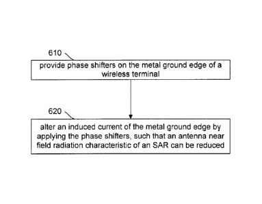
It can be learned from the aforementioned technical description that a general
thought for realizing SAR control may be as shown in Fig. 6. Referring to Fig.
6, which is
the flowchart for realizing SAR control according to an embodiment of the
disclosure, the
flow includes the following steps:
Step 610: phase shifters are provided on a metal ground edge of a wireless
terminal;
and
Step 620: an induced current of the metal ground edge is altered by applying
the
phase shifters, such that an antenna near field radiation characteristic of an
SAR can be
reduced.
To sum up, it can be seen that the technique for adding a plurality of phase
shifting
units on a PCB edge of a wireless terminal product provided by an embodiment
of the
disclosure may alter current phase and amplitude distribution of the metal
ground without
affecting the reception and transmission performance of the terminal, so as to
reduce a
local SAR peak value and lessen the harm of radiation to human bodies.
Furthermore,
the disclosure does not require any major change in a structure, circuit, and,
antenna of
a designed model, and can save space. The disclosure bears great flexibility
and
adaptability in an application, thereby realizing the objective of
miniaturized design of the
wireless terminal.
In addition, the disclosure does not impose any specific limitation on the
structures
8
CA 02825329 2013-07-22
and way of connection of the phase shifters. Adoption of other kinds of phase
shifter
circuit structures which are not mentioned in the disclosure falls in the
protection scope
of the disclosure. What described are only preferred embodiments of the
disclosure
and should not be used for limiting the protection scope of disclosure. Any
modification,
equivalent replacement, improvement, and the like made within the spirit and
principle of
the disclosure shall fall within the scope of protection of the disclosure.
9