Sélection de la langue

Search

Sommaire du brevet 2850529 

Énoncé de désistement de responsabilité concernant l'information provenant de tiers

Une partie des informations de ce site Web a été fournie par des sources externes. Le gouvernement du Canada n'assume aucune responsabilité concernant la précision, l'actualité ou la fiabilité des informations fournies par les sources externes. Les utilisateurs qui désirent employer cette information devraient consulter directement la source des informations. Le contenu fourni par les sources externes n'est pas assujetti aux exigences sur les langues officielles, la protection des renseignements personnels et l'accessibilité.

Disponibilité de l'Abrégé et des Revendications

L'apparition de différences dans le texte et l'image des Revendications et de l'Abrégé dépend du moment auquel le document est publié. Les textes des Revendications et de l'Abrégé sont affichés :

  • lorsque la demande peut être examinée par le public;
  • lorsque le brevet est émis (délivrance).
(12) Brevet: (11) CA 2850529
(54) Titre français: CARTE A ENSEMBLE ACTIF A BALAYAGE ELECTRONIQUE (AESA)
(54) Titre anglais: AN ACTIVE ELECTRONICALLY SCANNED ARRAY (AESA) CARD
Statut: Octroyé
Données bibliographiques
(51) Classification internationale des brevets (CIB):
  • H01Q 9/04 (2006.01)
  • H01Q 21/00 (2006.01)
(72) Inventeurs :
  • PUZELLA, ANGELO M. (Etats-Unis d'Amérique)
  • DUPUIS, PATRICIA S. (Etats-Unis d'Amérique)
  • LEMMLER, CRAIG C. (Etats-Unis d'Amérique)
  • BOZZA, DONALD A. (Etats-Unis d'Amérique)
  • BELLAHROSSI, KASSAM K. (Etats-Unis d'Amérique)
  • ROBBINS, JAMES A. (Etats-Unis d'Amérique)
  • FRANCIS, JOHN B. (Etats-Unis d'Amérique)
(73) Titulaires :
  • RAYTHEON COMPANY (Etats-Unis d'Amérique)
(71) Demandeurs :
  • RAYTHEON COMPANY (Etats-Unis d'Amérique)
(74) Agent: BERESKIN & PARR LLP/S.E.N.C.R.L.,S.R.L.
(74) Co-agent:
(45) Délivré: 2016-10-25
(86) Date de dépôt PCT: 2012-10-30
(87) Mise à la disponibilité du public: 2013-05-23
Requête d'examen: 2014-03-28
Licence disponible: S.O.
(25) Langue des documents déposés: Anglais

Traité de coopération en matière de brevets (PCT): Oui
(86) Numéro de la demande PCT: PCT/US2012/062542
(87) Numéro de publication internationale PCT: WO2013/074284
(85) Entrée nationale: 2014-03-28

(30) Données de priorité de la demande:
Numéro de la demande Pays / territoire Date
13/295,437 Etats-Unis d'Amérique 2011-11-14

Abrégés

Abrégé français

Selon un aspect, la présente invention concerne une carte à ensemble actif à balayage électronique (AESA) qui comprend une carte de circuits imprimés (PWB) qui comprend un premier ensemble de couches métalliques utilisé pour fournir une distribution de signaux RF, un deuxième ensemble de couches métalliques utilisé pour fournir une distribution logique numérique, un troisième ensemble de couches métalliques utilisé pour fournir une distribution de puissance et un quatrième ensemble de couches métalliques utilisé pour fournir une distribution de signaux RF. La PWB comprend au moins un canal d'émission/de réception (T/R) utilisé dans un AESA.


Abrégé anglais

In one aspect, an active electronically scanned array (AESA) card includes a printed wiring board (PWB) that includes a first set of metal layers used to provide RF signal distribution, a second set of metal layers used to provide digital logical distribution, a third set of metal layers used to provide power distribution and a fourth set of metal layers used to provide RF signal distribution. The PWB comprises at least one transmit/receive (T/R) channel used in an AESA.

Revendications

Note : Les revendications sont présentées dans la langue officielle dans laquelle elles ont été soumises.


1. An active electronically scanned array (AESA) card comprising.
a printed wiring board (PWB) comprising:
a first set of metal layers used to provide RF signal distribution,
a second set of metal layers used to provide digital logical distribution;
a third set of metal layers used to provide power distribution; and
a fourth set of metal layers used to provide RF signal distribution,
wherein the PWB comprises at least one transmit/receive (T/R) channel used in
an AESA.
2. The AESA card of claim 1 wherein the PWB further comprises.
a first composite layer of carbon fibers and epoxy between a metal layer of
the
second set of metal layers and a metal layer of the third set of metal layers;
and
a second composite layer of carbon fibers and epoxy between a metal layer of
the
third set of metal layers and a metal layer of the fourth set of metal layers
3. The AESA card of claim 2 wherein the PWB further comprises.
a layer of epoxy resin between two metal layers of the first set of metal
layers;
a layer of epoxy resin between two metal layers of the second set of metal
layers;
and
a layer of epoxy resin between two metal layers of the third set of metal
layers
4. The AESA card of claim 2 wherein the PWB further comprises a layer of
polyimide dielectric between two metal layers of the third set of metal
layers.
-9-

5. The AESA card of claim 1, further comprising one or more monolithic
microwave integrated circuits (MMICs) disposed on the surface of the PWB.
6. The AESA card of claim 1 wherein the MMICs are attached to the PWB using
solder balls.
7. The AESA card of claim 1 wherein the PWB further comprises:
a plurality of metal conduits, each electrical conduit coupling one of the
plurality
of layers to another one of the plurality of layers.
8. The AESA card of claim 7 wherein the PWB further comprises an RF via
having a first end coupled to a first metal conduit of the plurality of metal
conduits and a
second end opposite to the first end coupled to a second metal conduit of the
plurality of
metal conduits,
wherein the RF via extends through the third set of metal layers used for
power
distribution from the first set of metal layers used to provide RF signal
distribution to the
second set of metal layers used to provide didigital logical districution
without extending
through the fourth set of metal layers used to provide RF signal distribution.
9. The AESA card of claim 1 wherein the PWB further comprises:
a layer of epoxy resin between two metal layers of the first set of metal
layers;
a layer of epoxy resin between two metal layers of the second set of metal
layers;
a layer of epoxy resin between two metal layers of the third set of metal
layers;
and
-10-

a layer of polyimide dielectric between two metal layers of the third set of
metal
layers.
10. The AESA card of claim 1 wherein the AESA card does not include wire
bonds.
11 . An active electronically scanned array (AESA) assembly comprising:
an AESA card comprising:
a printed wiring board (PWB) comprising:
a first set of metal layers used to provide RF signal distribution;
a second set of metal layers used to provide digital logical distribution;
a third set of metal layers used to provide power distribution;
a fourth set of metal layers used to provide RF signal distribution; and
one or more monolithic microwave integrated circuits (MMICs) disposed on the
surface of the PWB,
wherein the PWB comprises at least one transmit/receive (T/R) channel used in
an AESA.
12. The ASEA assembly of claim 11, further comprising a cooling mechanism in
contact with the one or more of the MMICs.
13. The ASEA assembly of claim 12 wherein the cooling mechanism comprises:
a thermal heat spreader in contact with the MMICs; and
a cold plate in contact with the thermal spreader.
-11-

14. The ASEA assembly of claim 13 wherein the MMICs are attached to the
PWB using solder balls.
15. The ASEA assembly of claim 11 wherein the PWB further comprises:
a plurality of metal conduits, each electrical conduit coupling one of the
plurality
of layers to another one of the plurality of layers.
16. The ASEA assembly of claim 15 wherein the PWB further comprises a via
having a first end coupled to a first metal conduit of the plurality of metal
conduits and a
second end opposite to the first end connected to a second metal conduit of
the plurality
of metal conduits,
wherein the via extends through the third set of metal layers used for power
distribution from the first set of metal layers used to provide RF signal
distribution to the
second set of metal layers used to provide digital logical distribution
without extending
through the fourth set of metal layers used to provide RF signal distribution.
17. The ASEA assembly of claim 11 wherein the PWB further comprises:
a first composite layer of carbon fibers and epoxy between a metal layer of
the
second set of metal layers and a metal layer of the third set of metal layers;
and
a second composite layer of carbon fibers and epoxy between a metal layer of
the
third set of metal layers and a metal layer of the fourth set of metal layers.
18. The ASEA assembly of claim 17 wherein the PWB further comprises:
a layer of epoxy resin between two metal layers of the first set of metal
layers;
a layer of epoxy resin between two metal layers of the second set of metal
layers;
-12-

a layer of epoxy resin between two metal layers of the third set of metal
layers;
and
a layer of polyimide dielectric between two metal layers of the third set of
metal
layers.
19. The ASEA assembly of claim 11 wherein the AESA card does not include
wire bonds.
20. An active electronically scanned array (AESA) card comprising:
a printed wiring board (PWB) comprising:
a first set of metal layers used to provide RF signal distribution;
a second set of metal layers used to provide digital logical distribution;
a third set of metal layers used and to provide power distribution; and
a fourth set of metal layers used to provide RF signal distribution,
one or more monolithic integrated circuits (MMICs) disposed on the surface of
the PWB;
a plurality of metal conduits, each electrical conduit coupling one of the
plurality
of layers to another one of the plurality of layers; and
an RF via having a first end coupled to a first metal conduit of the plurality
of
metal conduits and a second end opposite to the first end coupled to a second
metal
conduit of the plurality of metal conduits,
wherein the RF via extends through the third set of metal layers used for
power
distribution from the first set of metal layers used to provide RF signal
distribution to the
second set of metal layers used to provide digital logical distribution
without extending
through the fourth set of metal layers used to provide RF signal distribution,
-13-

wherein the PWB comprises at least one transmit/receive (T/R) channel used in
an AESA, and
wherein the AESA card does not include wire bonds.
-14-

Description

Note : Les descriptions sont présentées dans la langue officielle dans laquelle elles ont été soumises.


CA 02850529 2016-02-12
AN ACTIVE ELECTRONICALLY SCANNED ARRAY (AESA) CARD
BACKGROUND
As is known in the art, a phased array antenna includes a plurality of active
circuits spaced apart from each other by known distances. Each of the active
circuits is
coupled through a plurality of phase shifter circuits, amplifier circuits
and/or other
circuits to either or both of a transmitter and receiver. In some cases, the
phase shifter,
amplifier circuits and other circuits (e.g., mixer circuits) are provided in a
so-called
transmit/receive (T/R) module and are considered to be part of the transmitter
and/or
receiver.
The phase shifters, amplifier and other circuits (e.g., T/R modules) often
require
an external power supply (e.g., a DC power supply) to operate correctly. Thus,
the
circuits are referred to as -active circuits- or -active components.-
Accordingly, phased
array antennas which include active circuits are often referred to as "active
phased
arrays." An active phased array radar is also known as an active
electronically scanned
array (AESA).
Active circuits dissipate power in the form of heat. High amounts of heat can
cause active circuits to be inoperable. Thus, active phased arrays should be
cooled. In
one example heat-sink(s) are attached to each active circuit to dissipate the
heat.
-1-

CA 02850529 2014-03-28
WO 2013/074284
PCT/US2012/062542
SUMMARY
In one aspect, an active electronically scanned array (AESA.) card includes a
printed 'iring board (MB) that includes a first set of metal layers -used to
provide RI'
signal distribution, a second set of metal layers used to provide digital
logical
distribution, a third set of metal layers used to provide power distribution
and a fourth set
of metal layers used to provide .11f signal distribution. The PWB comprises at
least one
transmit/receive (UR) channel used in an AESA.
In another aspect, an active electronically scanned array (AESA) assembly
includes an AESA card that includes a printed wiring board (PWB). The FW13
includes
a first set of metal la.yers used to provide RF signal distribution, a second
set of Instal
layers used. to provide digital logical distribution, a third sf.t of-metal
layers used to
provide power distribution and a fourth set of metal layers used to provide RF
signal
distribution. The AESA assembly also includes one or more monolithic microwave

integrated circuits (]Cs) disposed on the surface of the PW13. The PWB
includes at
least one transmit/receive (T/R) channei used. in an AESA.
DESCRIPTION OF Ti DRAWINGS
FIG. 1 A is a diagram of an active electronically scanned array (AESA) with an

array of active electronically scanned array (AESA) cards disposed en a mobile
platform.
FIG, 113 is a diagram of the array of AESA cards in FIG. IA.
FIG. 2 is a diagain Of an example of an AESA card with monolithic microwave
integrated drcuits (MMICs) disposed on the surface of the AESA card.
IC./. 3 is a cross-sectional view of an. AES.A assembly with an .AESA. card,
MMiCs and a cooling inechanism.
FIG. 4 is a cross-sectional view of a printed wiring board. (i).
-2-

CA 02850529 2014-03-28
WO 2013/074284
PCT/US2012/062542
DETAILED DESCRIPTION
Previous approaches to integrating active Monolithic Microwave Integrated
Circuits (.IC) for each active electronically scanned array (AESA)
Transmit/Receive
(ra) Chaimel included disposing these components in a metal container
(sometimes
called a "DR module"), which resdlts in an expensive assembly. In addition to
high
!material and test labor costs, extensive non-recurring engineering (RE) is
required for
changes in AES.,A. architecture (e.g., changes in active aperture size,
lattice changes,
number of DR channels per unit cell and so forth) or cooling approach. These
previous
approaches also 11{zie wire bonds that are used for radio frequency (RF),
power and logic
signals r the Tilt module; however, RF wire bonds can cause unwanted
electromagnetic coupling between UR channels or within a T/R channel.
Described herein is a new 'T/R. Channel architecture; an AESA card, The AESA
card reduces assembly reclining cost and test time and significantly reduces
'NU for
new applications or the integration of new MMIC technologies into AESA
applications.
17he AESA card may be fabricated using fully automated assembly process and
allows
for ease of modifying lattice dimensions and the number of TIR. channel cells
per
assembly, The .AESA card includes no wire bonds thereby significantly reducing
if not
eliminating electromagnetic coupling between T/R channels or within a T/R
charmel and
other electromagnetic interference (EMI). Thus, there is consistent channel-to-
channel
RF performance.
Referring to FIGS. ìA and 1 B, an AESA card may be used in a number of
applications. For example, as shown in FIG. IA, an array 12 of AESA cards 100
may be
used in a mobile environment such as in a mobile platfomi unit 10. In this
example, the
AES.A cards 100 are arranged in a 4 x 4 array, Though FIGS. 1A and I B depict
AESA
cards 100 that are in a shape of a rectangle, they may be constructed to be a
circle,

CA 02850529 2014-03-28
WO 2013/074284
PCT/US2012/062542
triangle or any polygon shape. Also, thou& the array 12 is in a shape of a
square the
array May be a rectangle; circle, triangle or any polygon arrangement.
Further, the
number of AESA cards 100 ma.y be one to any munber of AESA cards 100.
In other applications, one or more AESA. cards 100 may be used on the side of
naval vessels, on ground stractures and so forth. As witl be shown herein an
AESA card
100 is a "building block" to building an AESA system,
Referring to PIG. 2, an example of an AESA. card 100 is an AESA card 100' that
includes a printed wiring board (PWB) 101 and MMICs 104 (e.g., flip chips) on
a
surface of the PWB 101 (e.g., a surface 120 shown in FIG. 3). In this example,
the
-10 AESA card 100' includes a 4 x 8 array of Tilt channel cells 102 or 32
Tilt channel cells
102. Each TYR channel cell 102 includes the MMICs 1.04, a drain modulator 106
(e.g,, a
drain modulator integrated circuit (IC)), a limiter and low noise amplifier
(LNA) 108
(e.g., a gallium-arsenide (GaAs) I..NA with limiter), a power amplifier 110
(e.g., a
gallium-nitride (GaN) power amplifier). The AESA card 1.00' also includes one
or more
power and logic commtors 1 LI Tho.o. the T/R channel cells 102 are arranged in
a
rectangular array, the T/R channel cells 102 may be arranged in a. circle,
triangle or any
type of arrangement.
Referring to FIG. 3, an AESA assembly 150 includes an AESA card (e.g., an
AESA card 100") with the PWB 101 and MMICs 104 disposed on the surface 120 of
the
PWB 101 by solder balls 105, The .AES.A assembly 150 also includes a thermal
spreader
phne 160 coupled to each of the MICs through thennai epoxy 152 and a cold
plate
170. The cold plate 170 includes a channel 172 to receive a fluid such as a
gas or a
liquid to cool the MIkAICs 104. Thus, each MIMIC 104 is heat sunk in parallel.
That is,
the thermal resistance from the heat source (e.g., NEMICs 104) to the heat
sink (cold plate
170) is the same for all MMICs 104 and components (e.g., the drain modulator
106, the
-4.,.

CA 02850529 2014-03-28
WO 2013/074284
PCT/US2012/062542
LA 108, the power amplifier 110 and so forth) in each 'UR channel cell 102 Won
the
AESA card 100" thereby reducing the thermal gradient between T/R channel cells
1.02.
The AESA card 100" radiates RF signals in the R direction.
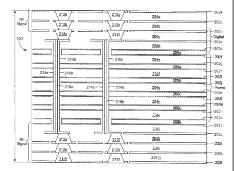
Referring to FIG. 4, an example of a printed wiring board (FW13) 101 is a PWB
101'. In one example, the thickness, t of the FWB 101' is about 64 mils.
The PWB 10P includes m.etal layers (e.g., metal layers 202a-202t) and one of
an
epoxy-resin layer (e.g., epoxy-resin layers 204a-204m), a polyimide dielectric
layer (e,g.,
polyimide dielectric layers 206a-206d) or a composite layer (e.g., composite
layers 208a,
208b) disposed between each of the metal layers (202a-202t). In particular,
the
composite layer 208a is disposed between the metal layers 210e, 210f and the
composite
ktyCT 208b is disposed between the metal layers 2100, 210p. The polyirnide
dielectric
layer 206a is disposed between the metal. layers 202g, 20211, the polyimide
dielectric
layer 206b is disposed between the metal layers 202i, 202j, the polyinaide
dielectric layer
206c is disposed between the metal layers 202k, 2021 and the polyimide
dielectric layer
20(d is dìspsed between the metal layers 202m, 202n. The remaining metals
layers
include an epoxy-resin layer (e.g., one of epoxy-resin layers 204a-204m)
disposed
between the metal layers as shown in FIG. 4.
The FWB 101 also includes RF vias (e.g., RF vias 210a, 210b) coupling the
metal layer 202d to the metal layer 202q. Each of the RF vias 210a, 210b
includes a pair
of metal plates (e.g., the RF via 210a includes metal plates 214a, 214h and
the RF via
210b includes metal plates 214e, 214d). The metal plates 214a, 214b are
separated by ari
epoxy resin 216a and the metal plates 2.14c, 214d are separated by an epoxy
resin 21.6b.
Though not shown in FIG. 4, one of ordinary skill in the art would recognize
that other
type vias exist for the digital logic layers and the power layers to bring
these signals to a
surface of the AESA card 100" or to other mend layers,

CA 02850529 2014-03-28
WO 2013/074284
PCT/US2012/062542
The PWB 101' also includes metal conduits (e.g., metal conduits 212a-212.1) to

electrically couple the RF vias 210a, 210b to the metal layers 202a, 202t. For
example,
the metal conduits 212a-212c are stacked one on top of the other with the
metal conduit
21:2a coupling the metal layer 202a to the metal layer 202b, the metal conduit
212b
coupling the metal layer 202h to the metal layer 202c and the metal conduit
212c
coupling the metal layer 202c to the metal layer 202d and to the RF via 210a.
The metal
conduits 212a-2121 are formed by chilling holes (e.g., about 4 or 5 mils in
diameter) into
the PWB 101' arid tilling the holes with a metal.
Further, the metal conduits 212d-212f are stacked one on top of the other with
th.e
metal conduit 212d coupling the metal layer 202r and the RF via 210a to the
metal layer
202s, the metal conduit 2.12e coupling the metal layer 202s to the metal layer
202t and
the metal conduit 212f coupling the metal layer 202t to the metal layer 202u.
The metal layers 2020-2020 and the epoxy-resin layers 204a-204b are used to
distribute RF signals. The metal layers 202p-202t, the epoxy-resin layers 204j-
204m are
also used to distribute RF signals. The metal layers 2020-202e and the epoxy-
resin
layers 204c-204d are used to distribute digital logic signals. The metal
layers 202f-202o,
the epoxy-resin layers 204e-204i and the polyimide dielectric layers 206a-206d
are used
to distribute power.
In one example, one or more of the metal layers 202a-202r includes copper.
f3ach
of metal layers 202a-202t may vary in thickness from about .53 mils to about
1.35 mils,
for example. In one example the RF vias 210a, 210b are made of copper. In one
example, the metal conduits 212a-2121 are made of copper
In one example, each of the epoxy-resin layers 204a-204m includes a high-
speedibigh performance epoxy-resin material compatible with. conventional FR-4
26 processing and has mechanical properties that make it a lead-free
assembly compatible to
-6-

CA 02850529 2014-03-28
WO 2013/074284
PCT/US2012/062542
include: a glass transition. temperature, îg, of about 200 C (Differentia
scanning
calorimetry (DSC)), a coefficient of thennal expansion (C ft) < îg 16, 1( &
55pp-110C
and CTE>Tg 18, 18 & 230ppneC. The low cm and a high Td (docmposifion
temperature) of 360 C are also advantageous in the sequential processing of
the stacked
metal conduits 212a-2121. Each of the epoxy-resin layers 204a-204m may vary in

thickness from about 5.6 mils to about 13.8 mils, for example. In one
particular
example, the t.Toxy-resin material is manufactured by Isola Group SARI under
the
product :Wale, FR408HR. in one example, the epoxy resin 216a, 216b is the
sarrie
material used for the epoxy-resin layers 204a-204m.
In one ex.ample, each of the polyimide dielectric layers 206a-206d includes a
polyitnide dielectric designed to film:lion as a power and ground plane in
printed circuit
boards for power bus decoupling and provides EMI and power plane impedance
reduction at high frequencies. In one example, each of the polyimide
dielectric layers is
about 4 MilS. In one. particular example, the polyinride dielectric is
manufacturod by
15 DUPONT under the product name, 11K-042536E.
In one example, each of the composite layers 208a, 208h includes a composite
of
epoxy resin and carbon fibers to provide CTE control and thermal management.
In one
example, the composite layers may be function as a ground plane and also may
function
as a mechanical restraining layer. In one example, each. of the composite
layers is about
20 1..8 mils, In one particular example, the composite of epoxy resin and
carbon fibers is
manufactured by STABLCORS Technology, Inc, under the product name, STIO-EP387.

In one example, the materials described above with respect to fabricating an
AESA card are lead-free. Thus, the solution proposed herein is meets
environmental
regulations rf...quiring products that are lead-free.
-7-

CA 02850529 2014-03-28
WO 2013/074284
PCT/US2012/062542
The processes described herein are not limited to the specific embodiments
described. Elements of different embodiments described herein may be combined
to
form other erribodiments not specifically set forth above. Other embodiments
not
specifically described herein are also within the scope of the following
claims.
Whitt is claimed is:
-8-

Dessin représentatif
Une figure unique qui représente un dessin illustrant l'invention.
États administratifs

Pour une meilleure compréhension de l'état de la demande ou brevet qui figure sur cette page, la rubrique Mise en garde , et les descriptions de Brevet , États administratifs , Taxes périodiques et Historique des paiements devraient être consultées.

États administratifs

Titre Date
Date de délivrance prévu 2016-10-25
(86) Date de dépôt PCT 2012-10-30
(87) Date de publication PCT 2013-05-23
(85) Entrée nationale 2014-03-28
Requête d'examen 2014-03-28
(45) Délivré 2016-10-25

Historique d'abandonnement

Il n'y a pas d'historique d'abandonnement

Taxes périodiques

Dernier paiement au montant de 263,14 $ a été reçu le 2023-09-20


 Montants des taxes pour le maintien en état à venir

Description Date Montant
Prochain paiement si taxe générale 2024-10-30 347,00 $
Prochain paiement si taxe applicable aux petites entités 2024-10-30 125,00 $

Avis : Si le paiement en totalité n'a pas été reçu au plus tard à la date indiquée, une taxe supplémentaire peut être imposée, soit une des taxes suivantes :

  • taxe de rétablissement ;
  • taxe pour paiement en souffrance ; ou
  • taxe additionnelle pour le renversement d'une péremption réputée.

Les taxes sur les brevets sont ajustées au 1er janvier de chaque année. Les montants ci-dessus sont les montants actuels s'ils sont reçus au plus tard le 31 décembre de l'année en cours.
Veuillez vous référer à la page web des taxes sur les brevets de l'OPIC pour voir tous les montants actuels des taxes.

Historique des paiements

Type de taxes Anniversaire Échéance Montant payé Date payée
Requête d'examen 800,00 $ 2014-03-28
Le dépôt d'une demande de brevet 400,00 $ 2014-03-28
Taxe de maintien en état - Demande - nouvelle loi 2 2014-10-30 100,00 $ 2014-03-28
Taxe de maintien en état - Demande - nouvelle loi 3 2015-10-30 100,00 $ 2015-10-05
Taxe finale 300,00 $ 2016-09-08
Taxe de maintien en état - Demande - nouvelle loi 4 2016-10-31 100,00 $ 2016-10-05
Taxe de maintien en état - brevet - nouvelle loi 5 2017-10-30 200,00 $ 2017-10-04
Taxe de maintien en état - brevet - nouvelle loi 6 2018-10-30 200,00 $ 2018-10-11
Taxe de maintien en état - brevet - nouvelle loi 7 2019-10-30 200,00 $ 2019-10-09
Taxe de maintien en état - brevet - nouvelle loi 8 2020-10-30 200,00 $ 2020-10-07
Taxe de maintien en état - brevet - nouvelle loi 9 2021-11-01 204,00 $ 2021-09-21
Taxe de maintien en état - brevet - nouvelle loi 10 2022-10-31 254,49 $ 2022-09-22
Taxe de maintien en état - brevet - nouvelle loi 11 2023-10-30 263,14 $ 2023-09-20
Titulaires au dossier

Les titulaires actuels et antérieures au dossier sont affichés en ordre alphabétique.

Titulaires actuels au dossier
RAYTHEON COMPANY
Titulaires antérieures au dossier
S.O.
Les propriétaires antérieurs qui ne figurent pas dans la liste des « Propriétaires au dossier » apparaîtront dans d'autres documents au dossier.
Documents

Pour visionner les fichiers sélectionnés, entrer le code reCAPTCHA :


Pour visualiser une image, cliquer sur un lien dans la colonne description du document. Pour télécharger l'image (les images), cliquer l'une ou plusieurs cases à cocher dans la première colonne et ensuite cliquer sur le bouton "Télécharger sélection en format PDF (archive Zip)" ou le bouton "Télécharger sélection (en un fichier PDF fusionné)".

Liste des documents de brevet publiés et non publiés sur la BDBC .

Si vous avez des difficultés à accéder au contenu, veuillez communiquer avec le Centre de services à la clientèle au 1-866-997-1936, ou envoyer un courriel au Centre de service à la clientèle de l'OPIC.


Description du
Document 
Date
(yyyy-mm-dd) 
Nombre de pages   Taille de l'image (Ko) 
Abrégé 2014-03-28 2 112
Revendications 2014-03-28 4 200
Dessins 2014-03-28 5 223
Description 2014-03-28 8 545
Dessins représentatifs 2014-03-28 1 79
Page couverture 2014-05-20 1 90
Revendications 2016-02-12 6 147
Description 2016-02-12 8 511
Dessins représentatifs 2016-10-05 1 58
Page couverture 2016-10-05 1 89
PCT 2014-03-28 4 185
Cession 2014-03-28 6 173
Demande d'examen 2015-09-14 3 213
Modification 2016-02-12 18 531
Taxe finale 2016-09-08 1 45