Note : Les descriptions sont présentées dans la langue officielle dans laquelle elles ont été soumises.
CA 02892333 2015-05-20
1
METHOD FOR CONVERTING ALTERNATING CURRENT INTO DIRECT CURRENT AND
RELATED DEVICE
Technical field and prior art
The invention relates to a method for converting alternating current into
direct
current, more commonly called AC/DC conversion, and the related conversion
device.
The invention applies, for example, to the electrical distribution for the
power
supply of loads of an aircraft. The converters that participate in such an
electrical
distribution first transform an alternative network into a direct network. The
alternative
network is, for example, a voltage network supplied by a generator external to
the
aircraft when the latter is on the ground. Using the direct network created as
such, other
converters, for example inverters, control the loads of the aircraft such as,
for example,
the starter for starting the auxiliary power unit located in the tail cone of
the aircraft.
To date, the energy conversion mode used to generate the direct network
operates in two successive steps, namely:
- a pre-load step during which an AC/DC conversion device is connected to the
three-phase alternative network by the intermediary of resistors, and
- a step of regulating the output voltage in order to raise the latter to a
desired
value.
The pre-load resistors limit the inrush current that occurs on the alternative
network when switching the converter to the network. During the pre-load,
there is no
regulation. The semiconductors that are part of the converter remain in
blocked state
and the converter is then equivalent to a three-phase diode bridge.
Figure 1 shows a global architecture of the AC/DC conversion device of prior
art
and figures 2A and 2B are detailed views of the device shown in figure 1.
The global architecture of the AC/DC conversion device comprises a block 1 of
pre-load resistors, a block 2 for AC/DC conversion, a decoupling capacitor 3,
a load 4 at
the terminals of which the direct voltage output Vdc is applied, a control
circuit 5, a set
of self-induction coils L1, L2, L3 with respective resistors r1, r2, r3, a
device Mv for
measuring alternating input voltages Va, Vb, Vc, a device Mc for measuring
input currents
CA 02892333 2015-05-20
2
IL2, IL3 that flow through the respective self-induction coils L1, L2, L3 and
a device MDC
for measuring the direct voltage output Vdc. The measurements output by the
devices
Mv, Mc and Mix are transmitted to the control circuit 5, which outputs the
settings CSG
which are applied to the AC/DC conversion block 2.
Figure 2A shows a detailed view of the block 1 of pre-load resistors. The
block 1
comprises three resistors R1, R2, R3 in series with three respective switches
Kll, K21, K31,
with the whole constituted of a resistor R, in series with a switch Ku (i=1,
2, 3) being
mounted in parallel of a switch Ki2.
Figure 2B shows a detailed view of the block 2 for AC/DC conversion. The block
2 comprises a three-phase bridge made of three arms in parallel, with each arm
being
made of two switches in series, with each switch being mounted in parallel of
a free-
wheeling diode. A first arm is formed from the switches Z1, Z2 and diodes D1,
D2. A
second arm is formed from switches Z3, Z4 and diodes D3, D4. A third arm is
formed from
switches Z5, Z6 and diodes D5, D6. Each switch Zi is provided with a control
terminal G;
(j=1, 2, ..., 6). Each arm has a middle point located between the two switches
in series
and whereon is applied a different alternating input voltage. The voltage Va
is as such
applied to the middle point of the switches Z1, Z2, the voltage Vb to the
middle point of
switches Z3, Z4 and the voltage Vc to the middle point of switches Z5, Z6. A
capacitor K is
mounted between the terminals where the output voltage Vdc is taken.
During the pre-load phase, the switches K11 (i=1, 2, 3) are conductive and the
switches Ki2 are in blocked state. The respective currents ILL, IL, IL3 then
flow through
the pre-load resistors R1, R2, R3. The resistors R1, R2 and R3 make it
possible to limit the
inrush current on the alternative network when switching the AC/DC converter
block to
the latter. During the entire pre-load step, the switches Z; are in blocked
state. The
output voltage Vdc rises to a value for the pre-load end voltage that is
theoretically
proportional to the effective value of the input voltage. When the output
voltage Vdc
reaches its theoretical value, the resistors R, (i=1, 2, 3) are short-
circuited by the closing
of the switches IQ (conductive state) and the regulation step is triggered.
During the
permanent state of the regulation step, the switches Zi are controlled
according to the
settings CSG in order to obtain the desired output voltage.
CA 02892333 2015-05-20
3
A disadvantage of this operating mode is the appearance of transient
phenomena of the inrush current type at the beginning of the regulation of the
output
voltage. This has for harmful consequences to stress the power components
(decrease in
the reliability and saturation of the inductances) and to prevent compliance
with
standards and requirements to be kept concerning the quality of the network.
Figures 3 and 4 show the appearance of these transient phenomena. Figure 3
shows the voltage Vdc at the output of the converter and figure 4 shows the
input
currents Ili (i=1, 2, 3) associated with these transient phenomena. It appears
in figure 4
that the inrush currents on the alternative network can reach, for example,
170A during
the transition between the pre-load step and the regulation step (instant to
in figures 3
and 4). In the case of N converters in parallel, the inrush current on the
input network is
multiplied by N. This results, for example, in an inrush current that can
reach 500A (case
with three converters in parallel). This is a real disadvantage.
The method of the invention does not have this disadvantage.
Disclosure of the invention
Indeed, the invention relates to a method for converting alternating current
into direct current implemented by a conversion device that comprises a three-
phase
bridge able to convert into direct voltage at least one alternating input
voltage, with the
three-phase bridge comprising at least one arm made of a first switch and of a
second
switch mounted in series, with each switch having a control input able to
control the
opening or the closing of the switch, with the method comprising a step of
regulating
the direct voltage, characterised in that it comprises a transition step which
precedes
the regulation step, with the transition step comprising the formation, using
the
alternating input voltage, of a first signal applied to the control input of
the first switch
and of a second signal applied to the control input of the second switch, in
such a way
that:
a) during the negative alternations of the alternating input voltage, the
first
signal is a pulse signal of which the width of the successive pulses widens
progressively
as a function of time, which opens and closes the first switch, and the second
signal is a
continuous signal that keeps the second switch open, and
CA 02892333 2015-05-20
4
b) during the positive alternations of the alternating input voltage, the
first
signal is a continuous signal that keeps open the first switch and the second
signal is a
pulse signal of which the width of the successive pulses widens progressively
as a
function of time, which opens and closes the second switch.
According to an additional characteristic of the method of conversion of the
invention, the formation, using the alternating input voltage, of said first
signal and of
said second signal comprises:
- a generation of successive pulses of which the width widens progressively
as a
function of time,
- a formation, using the alternating input voltage, of a level 1 logic signal
for the
positive alternations of the alternating input voltage and of level 0 for the
negative
alternations of the alternating input voltage,
- an inversion of the logic signal in order to form an inverted logic signal,
- a formation of the first signal using a first logic AND circuit that
receives on a
first input said pulses and on a second input the logic level signal, and
- a formation of the second signal using a second logic AND circuit that
receives
on a first input said pulses and on a second input the inverted logic signal.
The invention also relates to a device for converting alternating current into
direct current that comprises means able to implement the method of the
invention.
Brief description of the figures
Other characteristics and advantages of the invention shall appear when
reading a preferred embodiment made in reference to the annexed figures, among
which:
- Figure 1, already described, shows a global architecture of a AC/DC
conversion device;
- Figures 2A and 2B, already described, are detailed views of the device shown
in figure 1;
- Figures 3 and 4, already described, show the transient phenomena that
appear in an AC/DC converter of prior art during the transition between the
pre-load
step and the voltage regulation step;
CA 02892333 2015-05-20
- Figure 5 shows an AC/DC converter able to implement the method of the
invention;
- Figure 6 is a detailed view of the AC/DC converter shown in figure 5;
- Figures 7a, 7b and 7c show the formation of signals for controlling the
AC/DC
5 conversion device of the invention;
- Figures 8a and 8b show the operation of the circuits of the AC/DC conversion
device of the invention;
- Figures 9a, 9b and 9c show the operation of the AC/DC conversion device of
the invention under the effect of the control signals shown in figures 7a-7c.
Detailed disclosure of particular embodiments of the invention
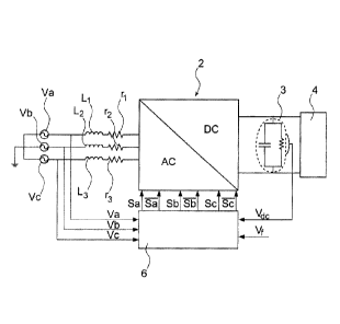
Figure 5 shows a converter of alternating current into direct current able to
implement the method of conversion of the invention.
In addition to the self-induction coils L1, L2, L3, of respective resistors
r1, r2, r3,
the conversion block 2 and the capacitor 3, the AC/DC converter comprises a
control
circuit 6.
The method of conversion of the invention comprises a transition step between
the pre-load step and the regulation step. It is the control circuit 6 that
allows for the
implementation of the transition step. The control circuit 6 is activated as
soon as the
pre-load step is terminated. The pre-load step terminates in a manner known
per se, for
example by timing or as soon as the direct voltage output reaches a
predetermined
threshold value.
As soon as it is activated, the control circuit 6 outputs control signals Sa,
Sa, Sb,
Sb, Sc, Sc which are applied, respectively, on the terminals G1-G6 of the
switches Z1-26.
The signals Sa and Sa are formed using the input voltage Va. Likewise, the
signals Sb
and Sb are formed using the input voltage Vb and the signals Sc and Sc are
formed
using the input voltage V. In order to avoid complicating figure 6, only the
generation of
the signals Sa and Sa using the input voltage Va is shown. However, in the
framework of
CA 02892333 2015-05-20
6
the invention, the control block also generates the signals Sb, Sb and Sc, Sc
according
to the same principle.
Figure 6 shows the control block 6 according to the preferred embodiment of
the invention. The bloc 6 comprises a first comparator 7 and a control signal
generation
block 8.
The control signal generation block 8 comprises:
- a pulse width modulator made of a carrier signal Vp generator 9, a ramp
signal
VR generator 10 and a comparator 11,
- a logic circuit 12,
- an inverter circuit 13, and
- two logic AND circuits 14 and 15.
The logic circuit 12 receives on its input the alternating voltage Va. The
logic
level at the output of the circuit 12 is equal to 1 when the voltage Va is
positive (positive
alternation) and to 0 when the voltage Va is negative (negative alternation).
This logic
level is applied to a first input of the AND circuit 14 and, after inversion
by the inverter
circuit 13, to a first input of the AND circuit 15, with the AND circuits 14
and 15 each
receiving the signal output by the comparator 11, which receives, on a first
input, the
carrier signal Vp output by the generator 9 and, on a second input, the ramp
signal Vp
output by the generator 10.
Figures 7a-7c show the formation of the control signals Sa, Sa which is
operated by the block 8 using the input signal Va.
Figure 7a shows the alternating input voltage Va. Figure 7b shows, in the same
mark, the carrier signal Vp and the ramp signal VR. The carrier signal Vp is,
for example, a
sawtooth voltage that varies between +1 and -1 with a frequency for example
equal to
15kHz. The symbolic levels +1 and -1 of the carrier signal Vp can correspond,
in practice,
to the respective voltage levels +5V and -5V. The voltage ramp signal VR is a
decreasing
signal of which the initial amplitude has a symbolic value equal to +1. In
practice, the
initial amplitude of the ramp signal corresponds to the maximum amplitude of
the
sawtooth signal, i.e., for example, +5V. Figure 7c shows, in the same mark,
the control
signals Sa and Sa output by the block 8.
CA 02892333 2015-05-20
7
It appears in figure 7c that:
- during positive alternations of the voltage Võ as soon as the amplitude of
the
carrier signal exceeds the value of the ramp voltage, the signal Sa is formed
of a
succession of rectangular pulses of which the width widens progressively while
the
signal Sa is at zero, and
- during negative alternations of the voltage Va, as soon as the amplitude of
the
carrier signal exceeds the value of the ramp voltage, the signal Sa is formed
of a
succession of rectangular pulses of which the width widens progressively while
the
signal Sa is at zero.
The truth table hereinbelow summarises the control logic of the arm which
comprises the switches Zb Z2:
Va>0 Va<0
Amplitude of VR less than Z1 blocked Z1 conductive
the amplitude of Vp Z2 conductive Z2 blocked
Amplitude of VR greater than Z2 blocked Z1 blocked
the amplitude of Vp Z1 blocked Z2 blocked
Figures 8a and 8b show the truth table mentioned hereinabove in reference to
the circuit.
Figures 9a-9c show the operation of the AC/DC conversion device of the
invention over all of the steps of operation, namely the pre-load step (I),
the transition
step (II) and the regulation step (III).
Figure 9a shows the output voltage Vdc of the AC/DC converter. Figure 9b shows
the current 114 that flows through the coil L1 at the input of the converter
and figure 9c
shows the ramp signal VR. For reasons of commodity, the currents IL2 and IL3
that flow
through the respective coils L2 and L3 are not shown in figures 9a-9c, with
these currents
having a variation that is similar to that of the current 114.
The inrush current IL1 is zero at the moment when the AC/DC converter
switches between the pre-load step (I) and the transition step (II). At the
beginning of
CA 02892333 2015-05-20
8
the transition step, the width of the rectangular pulses is low and the inrush
currents are
consequently of low amplitude. During the rest of the transition step, the
width of the
pulses increases with time and the inrush currents have an increasing
amplitude.
Likewise, the voltage Vdc which is measured at the output of the converter
increases (cf.
Figure 9a). During the transition step, the voltage Vdc measured at the output
of the
converter is compared by the comparator 7 with a predetermined threshold value
Vf
equal, for example, to 90% of the regulation direct voltage desired. As soon
as the
voltage Vdc reaches the value Vf, the comparator 7 outputs a comparison signal
which
interrupts the transition step and triggers the regulation step.
The duration AT of the transition step is advantageously adjustable. An
advantage of the adjustable nature of the duration AT is to be able to vary
the duration
of the time for the increase in the voltage Vdc. In figures 9a-9c, it appears
that this
duration is, for example, equal to 80ms.
Advantageously, the inrush currents IL, (1=1, 2, 3) have an amplitude that
remains low all throughout the transition step and during the starting of the
regulation
step. By way of a non-restricted example, as shown in figure 9b, the value of
the current
IL1 varies from substantially OA to substantially 40A between the starting of
the
transition step and the starting of the regulation step.