Note : Les descriptions sont présentées dans la langue officielle dans laquelle elles ont été soumises.
LCD SOURCE DRIVER FEEDBACK SYSTEM AND METHOD
Inventors: Charles Lemons, Gary Baek, Steve Preston, and David Williams
Cross-Reference to Related Applications
[0001] This application claims priority to US Application No. 81/805,784 filed
on March
27, 2013.
Technical Field
[0002] The disclosed embodiments of the present invention relate to an LCD
source
driver assembly using dummy feedback channels.
Background of the Art
[0003] LCD assemblies contain a plurality of components that may fail
overtime. This
can be undesirable in many different situations but specifically when the LCD
is being
used for information purposes within critical applications (such as
instrumentation for
fixed wing or rotary wing aircraft, ground vehicles, mission control, etc.).
At times there
are concerns that the LCD display is not being updated accurately due to a
failure in the
source driver.
Summary of the Preferred Embodiments of the Invention
[0004] In an exemplary embodiment, dummy channels may be placed on the source
driver and can be driven with known values. The output of these source driver
channels
1
STL-SDF/PCT-CDA
CA 2908700 2018-01-11
can then be compared to the known values to determine if the source driver is
functioning properly.
[0005] In an aspect, there is provided a method for detecting a failure in an
LCD
source driver comprising the steps of:
providing at least one dummy channel in addition to a number of active
channels
on the source driver;
driving the dummy channel and all of the active channels to be used with
original
signals;
receiving the dummy channel original signal at a microprocessor; and
comparing said dummy channel original signal with at least one active channel
original signal at the microprocessor.
[0006] In another aspect, there is provided an electrical assembly for
detecting failures
in an LCD source driver comprising a plurality of active channels on the
source driver
which communicate electronically with an LCD. A dummy channel is on the source
driver which is driven with an original signal, and a microprocessor receives
the dummy
channel and compares the received dummy channel signal to the original signal,
wherein the dummy channel is configured to bypass the LCD.
Brief Description of the Drawings
[0007] A better understanding of the disclosed embodiments will be obtained
from a
reading of the following detailed description and the set of accompanying
drawings.
[0008] FIGURE 1 provides a schematic of a traditional LCD assembly.
[0009] FIGURE 2 provides a schematic of a traditional LCD source driver
architecture.
STIADF/PCT-CDA
CA 2908700 2018-12-20
[0010] FIGURE 3 provides a schematic of an exemplary embodiment of the LCD
source driver feedback system.
[0011] FIGURE 4 provides a schematic of an alternative embodiment of the LCD
source driver feedback system.
[0012] FIGURE 5 provides a schematic of an alternative embodiment of the LCD
source driver feedback system.
[0013] FIGURE 6 provides a logical flowchart for one embodiment of the method.
[0014] FIGURE 7 provides a logical flowchart for another embodiment of the
method.
Detailed Description of a Preferred Embodiment
[0015] The invention is described more fully hereinafter with reference to the
accompanying drawings, in which exemplary embodiments of the invention are
shown.
This invention may, however, be embodied in many different forms and should
not be
construed as limited to the exemplary embodiments set forth herein. Rather,
these
embodiments are provided so that this disclosure will be thorough and
complete, and
will fully convey the scope of the invention to those skilled in the art. In
the drawings, the
size and relative sizes of layers and regions may be exaggerated for clarity.
[0016] It will be understood that when an element or layer is referred to as
being "on"
another element or layer, the element or layer can be directly on another
element or
layer or intervening elements or layers. In contrast, when an element is
referred to as
being "directly on" another element or layer, there are no intervening
elements or layers
present. Like numbers refer to like elements throughout. As used herein, the
term
"and/or" includes any and all combinations of one or more of the associated
listed items.
3
STIADF/PCT-CDA
CA 2908700 2018-01-11
[0017] It will be understood that, although the terms first, second, third,
etc., may be
used herein to describe various elements, components, regions, layers and/or
sections,
these elements, components, regions, layers and/or sections should not be
limited by
these terms. These terms are only used to distinguish one element, component,
region,
layer or section from another region, layer or section. Thus, a first element,
component,
region, layer or section discussed below could be termed a second element,
component, region, layer or section without departing from the teachings of
the present
invention.
[0018] Spatially relative terms, such as "lower", "upper" and the like, may be
used
herein for ease of description to describe the relationship of one element or
feature to
another element(s) or feature(s) as illustrated in the figures. It will be
understood that
the spatially relative terms are intended to encompass different orientations
of the
device in use or operation, in addition to the orientation depicted in the
figures. For
example, if the device in the figures is turned over, elements described as
"lower"
relative to other elements or features would then be oriented "upper" relative
the other
elements or features. Thus, the exemplary term "lower" can encompass both an
orientation of above and below. The device may be otherwise oriented (rotated
90
degrees or at other orientations) and the spatially relative descriptors used
herein
interpreted accordingly.
[0019] The terminology used herein is for the purpose of describing particular
embodiments only and is not intended to be limiting of the invention. As used
herein, the
singular forms "a", "an" and "the" are intended to include the plural forms as
well, unless
the context clearly indicates otherwise. It will be further understood that
the terms
4
$11-$DF/PCI-CDA
CA 2908700 2018-01-11
"comprises" and/or "comprising," when used in this specification, specify the
presence of stated features, integers, steps, operations, elements, and/ or
components,
but do not preclude the presence or addition of one or more other features,
integers,
steps, operations, elements, components, and/or groups thereof.
[0020] Embodiments of the invention are described herein with reference to
cross-
section illustrations that are schematic illustrations of idealized
embodiments (and
intermediate structures) of the invention. As such, variations from the shapes
of the
illustrations as a result, for example, of manufacturing techniques and/or
tolerances, are
to be expected. Thus, embodiments of the invention should not be construed as
limited
to the particular shapes of regions illustrated herein but are to include
deviations in
shapes that result, for example, from manufacturing.
[0021] For example, an implanted region illustrated as a rectangle will,
typically, have
rounded or curved features and/or a gradient of implant concentration at its
edges
rather than a binary change from implanted to non-implanted region. Likewise,
a buried
region formed by implantation may result in some implantation in the region
between
the buried region and the surface through which the implantation takes place.
Thus, the
regions illustrated in the figures are schematic in nature and their shapes
are not
intended to illustrate the actual shape of a region of a device and are not
intended to
limit the scope of the invention.
[0022] Unless otherwise defined, all terms (including technical and scientific
terms)
used herein have the same meaning as commonly understood by one of ordinary
skill in
the art to which this invention belongs. It will be further understood that
terms, such as
those defined in commonly used dictionaries, should be interpreted as having a
STL-SDF/PCT-CDA
CA 2908700 2018-01-11
meaning that is consistent with their meaning in the context of the relevant
art and will
not be interpreted in an idealized or overly formal sense unless expressly so
defined
herein.
[0023] FIGURE 'I provides a schematic of a traditional LCD assembly, The
display
interface board (DIB) preferably contains the necessary electronics to control
the source
and gate drivers,
[0024] FIGURE 2 provides a schematic of a traditional LCD source driver
architecture.
Each source driver typically has 'n' number of channels to drive the red,
green, and blue
sub-pixels on each line of the LCD. Of course, it is known to use other
combinations of
sub-pixels in some applications, such as more than one of each red, green, and
blue or
sometimes an additional sub-pixel color such as yellow. The preferred
embodiments
herein can be used with any combination and colors for the LCD sub-pixels. The
red,
green, and blue are the most widely used combination, so this is shown here.
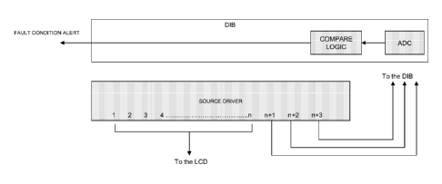
[0025] FIGURE 3 provides a schematic of an exemplary embodiment of the LCD
source driver feedback system. As an example, assume that the source driver is
capable of driving 960 channels or 320 (960/3) pixels (a pixel in this
embodiment is
comprised of a red, green, and blue sub-pixels). If only 957 channels are used
to drive
the LCD, then 3 channels may be available for data integrity checking of the
source
driver. These 3 channels, referred to as "dummy channels" since they are not
connected to the LCD, can be routed back to the DIB where they can be
digitized
(converted from an analog signals to a digital signal) and compared to the
known or
driven data. It should be noted that although three dummy channels are shown
here,
three are not required. As few as one. or two dummy channels can be used, or
6
STL-SDF/PCT-CDA
CA 2908700 2018-01-11
alternatively more than three dummy channels could be used. The 'DIB' as used
herein
refers to a display interface board which is commonly used in LCD
applications.
Generally speaking, these are printed circuit boards with several electronic
components,
most notably a microprocessor for operating the logic described throughout
this
application.
[0028] For instance, say the DIB provided a digital value of 255(d) for sub-
pixel N+1,
digital value of 64(d) for sub-pixel N+2, and a digital value of 128(d) for
N+3. The
source driver may convert these digital values to a corresponding analog
voltage based
on gamma and polarity. The analog voltages from N+1, N+2, and N+3 would
preferably
be routed back to the DIB where they would be digitized and compared against
the
driven digital values. If the two values match, then one could assume, with a
high level
of confidence that the source driver is functioning properly. If the two
values do not
match, then one could assume, with a high level of confidence that the source
driver is
not functioning properly. If multiple mismatches do occur, then the DIB may
alert the
control logic upstream that an error condition has been detected. The action
taken by
the DIB under a fault condition could be any one of many actions, such as but
not
limited to: driving the LCD black, display text on the LCD indicating a fault
condition has
occurred, audible warnings, flashing lights or LEDs positioned near the LCD,
or any
other number of possibilities.
[0027] FIGURE 4 provides a schematic of an alternative embodiment of the LCD
source driver feedback system. There are of course many combinations for
connecting
the 'dummy' channels out of a source driver and back to the DIB. In this
embodiment,
the figure shows dummy channels on each end of the source driver. While this
=
7
sit-sDF/PCT-CDA
CA 2908700 2018-01-11
embodiment shows three dummy channels on each end of the source driver, there
is no
requirement that the number of dummy channels on each end of the source driver
is
equal, as they could be different.
[0028] FIGURE 5 provides a schematic of an alternative embodiment of the LCD
source driver feedback system. This figure illustrates a situation where there
may not be
any dummy channels available out of the source driver. In this situation,
original signals
sent to active LCD channels may be split and routed back to a microprocessor
on the
DIB as a dummy split channel. In this situation, it would be preferable if the
original
signal sent to the split active channel was a signal for the image to be
produced on the
LCD. Again, while the embodiment shown uses the last three sub-pixels out of
the
source driver to perform the integrity check, this is not required. As few as
one channel
could be used or as many as hundreds of channels could be used. Also, this
splitting
technique could be used in combination with the designated dummy channel
technique
shown above in Figures 3 and 4.
[0029] FIGURE 6 provides a logical flowchart for one embodiment of the method.
Here, at least one dummy channel is initially provided and is driven with an
original
signal. The resulting signal from the dummy channel is then received as a
received
dummy channel signal. Here, the DIB or other PCB containing a microprocessor
would
contain the comparison logic which would preferably compare the received dummy
channel signal with the original dummy channel signal. If the two match, the
logic
returns to drive the dummy channel with another original signal to repeat the
process. If
the two do not match, an error is sent upstream to notify the user as to an
error..
8
STL-SDF/PCT=CDA
CA 2908700 2018-01-11
[0030] FIGURE 7 provides a logical flowchart for another embodiment of the
method.
In this embodiment, an active channel is initially split to produce a dummy
channel and
an active channel. Both the dummy channel and the active channel are then
driven with
the same original signal. The active channel is then sent to the LCD while the
dummy
channel is received as a received dummy channel signal. Again, this received
dummy
channel signal is then compared with the original signal to determine if an
error has
occurred.
[0031] Having shown and described a preferred embodiment of the invention,
those
skilled in the art will realize that many variations and modifications may be
made to
affect the described invention and still be within the scope of the claimed
invention.
Thus, many of the elements indicated above may be altered or replaced by
different
elements which will provide the same result and fall within the spirit of the
claimed
invention. It is the intention, therefore, to limit the invention only as
indicated by the
scope of the claims.
9
STL=SDF/PCT-CDA
CA 2908700 2018-01-11