Note : Les descriptions sont présentées dans la langue officielle dans laquelle elles ont été soumises.
CA 02927067 2016-04-12
WO 2015/074754
PCT/EP2014/003097
Method for transmittinn a USB signal and
USB transmission system
The invention relates to a method for transmitting three data signals of a USB
signal in
which the first data signal is transmitted differentially via a first
conductor pair and the
second data signal is transmitted differentially via a second conductor pair.
The invention
also relates to a system for transmitting USB signals and an adapter for such
a system.
Conventional USB2 interfaces (for example USB 2.0 interfaces) have a signal
conductor
pair (D+ and D-) and a conductor pair for the power supply (GND, VBUS). The
data
transmission takes place symmetrically and bidirectionally via the signal
conductor pair,
whereby the data signal ("signal portion") is transmitted through one
conductor of the
signal conductor pair and the corresponding inverted data signal ("reference
portion") is
transmitted through the other conductor. For this purpose a cable designed for
the
transmission of USB2 signals has, as a signal conductor pair, two twisted and
shielded
conductors in order as far as possible to avoid transmission interference. The
signal
receiver forms the differential voltage of the data signal transmitted via the
signal
conductor pair differentially (namely symmetrically), so that interference
affecting both
conductors of the signal conductor pair equally is eliminated.
The transmission of USB signals is necessary in an extremely wide variety of
technical
applications. For example, a USB socket can be required in a rear section of a
vehicle in
order to allow USB devices to be plugged in, so that a USB cable needs to be
passed
CA 02927067 2016-04-12
WO 2015/074754
PCT/EP2014/003097
-2-
through the vehicle from the front to the rear. USB sockets or USB connections
can also
be required in various locations (offices, public facilities, means of
transport etc.) for the
connection of USB devices, whereby USB cables need to be laid for this
purpose. As
explained above, two conductor pairs are sufficient for the transmission of a
conventional
USB2 signal (data signal and supply voltage), so that four-wire cables were
formerly laid
for the transmission of USB signals.
A few years ago, the USB3 standard was introduced. USB3 interfaces (for
example USB
3.0 interfaces) have, in addition to the aforementioned connections (D+, D-,
GND,
VBUS), at least two additional signal conductor pairs (SSTX+ and SSTX-; SSRX+
and
SSRX-). A differential data signal is transmitted or fed into the USB
interface via each of
these two signal conductor pairs. Overall, this allows higher data rates to be
achieved
than with the conventional USB2 standard.
Consequently, in order to achieve USB3 compatibility, new plug connectors on
the host
and on the connected devices and additional data transmission cables are
necessary.
For this purpose, a further four-wire cable was laid for the transmission of
USB3 signals,
whereby the aforementioned eight USB3 connections (D+, D-, GND, VBUS, SSTX+
and
SSTX-; SSRX+ and SSRX-) are then transmitted via two four-wire cables. The
total of
three data signals are thereby transmitted differentially via in each case one
conductor
pair (D+ and D-; SSTX+ and SSTX-; SSRX+ and SSRX-). However, the laying of
additional cables involves considerable expense.
Alternatively, instead of the two four-wire cables, it is naturally possible
to lay a single
standard USB3 cable. However, laying such a cable involves even greater
expense,
since the old USB2 cables need to be removed and the new USB3 cables are
expensive.
In view of the described problems it is the object of the present invention to
provide a
method for transmitting USB signals with at least three data signals which
requires less
expense and fewer changes than the conventional method.
This problem is essentially solved in that a signal portion of the third data
signal is
transmitted as a common mode component via the first conductor pair and a
reference
CA 02927067 2016-04-12
WO 2015/074754
PCT/EP2014/003097
-3-
portion of the third data signal is transmitted as a common mode component via
the
second conductor pair.
In other words, the three data signals which are to be transmitted
differentially are
transmitted not via the three conductor pairs which are, properly speaking,
necessary,
but via only two conductor pairs. Cables with two wire pairs are already laid
in numerous
technical applications, for example in vehicles, offices etc., so that no
additional cables
need to be laid for the desired transmission of the three USB3 data signals.
The supply signal which is additionally necessary in order to supply voltage
to the USB
device can usually be fed more simply by other means, without additional
cables
needing to be laid. For example, in automobiles a d.c. voltage supply is in
any case
available in a wide variety of locations which can readily be used. Moreover,
unlike
conductor pairs used for the transmission of data signals, the conductor pair
used for the
transmission of the supply voltage does not require complete shielding, nor
symmetrical
and even twisting etc., so that if necessary an additional cable for providing
the supply
voltage can be laid.
The invention is based on the knowledge, originating from the field of
analogue
telephony, that under certain conditions three differential data signals can
be transmitted
via only two conductor pairs, namely when the third data signal is transmitted
via a so-
called phantom circuit. For this purpose, the signal portion of the third data
signal which
corresponds to the inverted reference portion of the third data signal, or a
multiple or a
fraction thereof (preferably half the signal portion D+12) is transmitted as a
common
mode component via the first signal conductor pair and the reference portion
of the third
data signal which corresponds to the inverted signal portion, or a multiple or
a fraction
thereof (preferably half the reference portion D-/2) is transmitted as a
common mode
component via the second signal conductor pair.
In other words, prior to transmission, the signal portion of the third data
signal can be
added, as a common mode component, to the first data signal which is to be
transmitted
differentially, and the reference portion of the third data signal can be
added, as a
common mode component, to the second data signal which is to be transmitted
differentially.
CA 02927067 2016-04-12
WO 2015/074754
PCT/EP2014/003097
-4-
Following transmission, the third data signal can be assembled from the common
mode
component of the signal transmitted via the first conductor pair and the
common mode
component of the signal transmitted via the second conductor pair as a
differential data
signal. The first data signal and the second data signal are not affected by
the
transmission of the third data signal via the same conductors, since the
signal portions
and reference portions of the first and second data signals are in each case
shifted by
the same amount (in the common mode), so that the difference, which represents
the
actual data stream, remains unchanged. This principle is fundamentally known
from the
field of analogue telephony, and in this respect reference is made to the
relevant
technical literature.
In view of the low susceptibility to interference, it has thereby proved
advantageous for
the first data signal, the second data signal and/or the third data signal to
be fed in
symmetrical form before the step of adding the common mode component. In other
words, the signal portions of the differentially fed USB signals correspond in
each case
to the inverted reference portions. In particular, the signal portion of the
third data signal
transmitted in common mode via the first signal conductor pair corresponds in
amount to
the reference portion of the third data signal transmitted in common mode via
the second
signal conductor pair, whereby, however, the signal portion and reference
portion have
opposite signs.
In order to protect the data signals against external interference through
electromagnetic
interference fields, the two conductor pairs can be shielded by means of a
common
shielding.
A particularly low-interference transmission is possible if the two conductor
pairs are laid
in a star quad arrangement, preferably in the form of an HSD transmission
system. The
HSD transmission system carries two symmetrical conductor pairs in a cable.
Both pairs
are surrounded by a common shield. The individually insulated conductors are
thereby
arranged in the form of a star quad and can be twisted together. Two
conductors
arranged opposite one another in the star quad form a common differential wire
pair.
This means that there is always a symmetrical pair in the virtual ground plane
of the
respective second pair. This makes it possible to realise a high crosstalk
attenuation
while at the same time keeping the cable as compact as possible.
CA 02927067 2016-04-12
WO 2015/074754
PCT/EP2014/003097
The method according to the invention is particularly suitable for the
transmission of a
USB3 signal, for example a USB 3.0 signal, whereby the USB3 data are
transmitted
from the host to the device (SSTX+ and SSTX-) via the first conductor pair and
the
USB3 data are transmitted from the device to the host (SSRX+ and SSRX-) via
the
second conductor pair, while the D+/D- signal is transmitted via the phantom
circuit.
A further aspect of the invention relates to a USB signal transmission system
with two
adapters which are connected together via two pairs of transmitter signal
conductors,
whereby each of the adapters has a USB interface for the input/output of a USB
signal.
According to the invention, the USB interfaces in each case have at least
three pairs of
USB signal conductors which are in each case configured for the differential
transmission of a USB data signal. The three pairs of USB signal conductors
are coupled
with the two pairs of transmitter signal conductors via a phantom circuit.
In other words the adapters in each case possess means for adding a first
common
mode component to the differential signal fed via the first USB signal
conductor pair in
order to generate a first differential transmission signal for transmission
via the first
transmitter signal conductor pair and means for adding a second common mode
component to the differential signal fed via the second USB signal conductor
pair in
order to generate a second differential transmission signal for transmission
via the
second transmitter signal conductor pair, whereby the first common mode
component
corresponds to a signal portion of the differential signal fed via the third
USB signal
conductor pair or a multiple or fraction thereof and the second common mode
component corresponds to a reference portion of the differential signal fed
via the third
USB signal conductor pair or the multiple or the fraction thereof.
The USB signal transmission system according to the invention thus has in each
case
three conductor pairs as input and output, each conductor pair being
configured for the
transmission of a differential USB data signal, while the transmission itself
takes place
via only two conductor pairs. The third USB data signal is transmitted via the
third
conductor pair provided via the phantom circuit.
CA 02927067 2016-04-12
WO 2015/074754
PCT/EP2014/003097
-6-
Preferably, the first USB signal conductor pair is an SSTX signal conductor
pair (SSTX+
and SSTX-), the second USB signal conductor pair is an SSRX signal conductor
pair
(SSRX+ and SSRX-) and the third USB signal conductor pair is a D signal
conductor pair
(D+ and D-). The data signal transmitted via the D signal conductor pair is
thus
transmitted as a virtual signal.
In terms of achieving a low-interference transmission, it has proved
advantageous for the
two pairs of transmitter signal conductors to be arranged in a star quad form
and
preferably designed as an HSD connection. For this purpose, the two adapters
are
advantageously connected by means of a star quad cable. Alternatively or in
addition,
HSD plug connectors in the form of HSD sockets or similar can be arranged at
the
adapter outputs connected with one another via the transmitter signal
conductors, said
plug connectors being connected with one another via a star quad cable or
another
cable with at least two conductor pairs.
In addition, a supply conductor pair can run between the two adapters which
may be
connected with supply conductor pairs of the USB interfaces.
It is practical for a USB3 connection socket and/or a USB3 connection cable to
be
connected to at least one of the USB interfaces.
The susceptibility to interference of the USB data signals which are to be
transmitted can
be reduced through an electromagnetic shielding starting out from the first
USB interface
and running via both adapters and the transmitter signal conductor pairs up to
the
second USB interface for electromagnetic shielding of the data signals.
In conventional phantom circuits, coils are often present in which the common
mode
component is added to the differential first and second data signals by
feeding the
phantom currents (signal portion and reference portion of the third
differential data
signal) into the secondary centres. As a result, the magnetic effects cancel
one another
out and the phantom currents do not induce any voltage on the primary sides of
the
coils.
CA 02927067 2016-04-12
WO 2015/074754
PCT/EP2014/003097
-7-
Alternatively, the phantom circuits can be realised through digital switching
elements in
the adapters, for example through circuit boards arranged in each of the
adapters
containing logical switching elements such as digital addition and/or
subtraction.
According to a particularly important aspect of the invention, an adapter for
a USB signal
transmission system is provided which has a first interface for the
input/output of a USB
signal and a second interface, in particular an HSD interface. The first
interface is
designed in the form of a USB interface with three USB signal conductor pairs,
each pair
being configured for the differential transmission of a USB data signal, and
the second
interface has two transmitter signal conductor pairs, each pair being
configured for the
differential transmission of a data signal. According to the invention, the
adapter is
equipped with means for adding a first common mode component to the
differential
signal which is to be fed via the first USB signal conductor pair in order to
generate a first
differential transmission signal for transmission via the first transmitter
signal conductor
pair, and means for adding a second common mode component to the differential
signal
which is to be fed via the second USB signal conductor pair in order to
generate a
second differential transmission signal for transmission via the second
transmitter signal
conductor pair, whereby the first common mode component corresponds to a
signal
portion of the differential signal which is to be fed via the third USB signal
conductor pair
or a multiple or a fraction thereof and the second common mode component
corresponds to a reference portion of the differential signal which is to be
fed via the third
USB signal conductor pair or a multiple or fraction thereof.
In a particularly preferred embodiment, the second interface is an HSD
interface. A
USB3 socket (for example a USB 3.0 socket) and/or a USB3 cable (for example a
USB
3.0 cable) can be connected to the USB interface. An HSD socket, an HSD plug
connector and/or an HSD cable can be connected to the second interface.
In the following description, the invention is explained with reference to the
attached
drawing, in which:
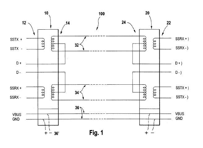
Fig. I shows a schematic circuit plan of a USB transmission system according
to
the invention which is suitable for carrying out the method according to the
invention.
CA 02927067 2016-04-12
WO 2015/074754
PCT/EP2014/003097
-8-
The USB transmission system 100 has in total two adapters 10 and 20 according
to the
invention. Each adapter 10, 20 has on one side a conventional USB3 interface
12, 22
(for example a USB 3.0 interface) and on the other side a second interface 14,
24 which
has two signal conductor pairs 32, 34 for the differential transmission of
data signals.
The second interface can in each case be, for example, an HSD interface.
The second interfaces 14, 24 of the two adapters 10, 20 can be connected with
a cable
in which two, in each case twisted, conductor pairs run, for example in the
manner of a
star quad arrangement. The two conductor pairs can in each case be shielded.
Preferably, the cable with the two conductor pairs 32, 34 has an outer
conductor as
common shield.
The two adapters 10, 20 can be connected by means of a further conductor pair
36
carrying a supply voltage (for example 5V d.c. voltage). However, this further
conductor
pair 36 is not essential to the invention, and a supply voltage 36' can also
be fed
externally to one or two USB interfaces 12, 24, for example through the
voltage supply
which is in any case present in an automobile.
Each of the two USB interfaces has the usual USB3 connections SSTX+, SSTX-;
SSRX+, SSRX-; D+, D-. A first differential data signal can be fed to the
connection pair
SSTX+, SSTX-, the signal portion of which is referred to in the following as
SSTX+ and
its reference portion referred to in the following as SSTX-. USB signals are
normally
transmitted symmetrically. The difference between SSTX+ - SSTX- represents the
actual
data stream. If the absolute values of the voltages of the signals SSTX+ and
SSTX- shift
by the same amount due to interference, the difference between the values
remains
unchanged.
A second differential data signal can be fed to the connection pair SSRX+,
SSRX-, the
signal portion of which is referred to in the following as SSRX+ and its
reference portion
referred to in the following as SSRX-.
A third differential data signal can be fed to the connection pair D+, D- ,
the signal
portion of which is referred to in the following as D+ and its reference
portion referred to
in the following as D-.
CA 02927067 2016-04-12
WO 2015/074754
PCT/EP2014/003097
-9-
The signal portion D+ of the third differential signal is transmitted as a
common mode
component via the transmitter signal pair 32. This means the signals
(SSTX+)+(D+/2)
and (SSTX-)+(D+/2) are transmitted via the first signal pair 32. The
difference between
these signals produces (SSTX+)-(SSTX-) and thus the data stream of the first
data
signal. The total of these signals produces (SSTX+)+(SSTX-)+(D+)=(D+), since
(SSTX+)=-(SSTX-).
The reference portion D- of the third differential signal is transmitted as a
common mode
component via the transmitter signal pair 34. This means the signals
(SSRX+)+(D-/2)
and (SSRX-)+(D-/2) are transmitted via the second signal pair 34. The
difference
between these signals produces (SSRX+)-(SSRX-) and thus the data stream of the
second data signal. The total of these signals produces (SSRX+)+(SSRX-)+(D-ND-
),
since (SSRX+)=-(SSRX-).
Possible sources of interference acting as a common mode signal on both
transmitter
signal pairs 32, 34 are eliminated in the subtraction (D+)-(D-).
According to the invention it is thus possible to transmit three USB data
signals
differentially via only two conductor pairs. Through the use of the adapters
according to
the invention at the two ends of the cables with two conductor pairs which are
already
laid in numerous technical applications, USB3 signals can thus be transmitted
without
any need to lay additional cables.
The adapter according to the invention for use in the USB transmission system
according to the invention can be realised in the form of a circuit board with
digital
switching elements such as addition and/or subtraction, whereby a USB3 socket
can be
coupled to the USB interface of the adapter and an HSD plug connector and/or a
star
quad cable can be coupled to the second interface of the adapter.