Note : Les descriptions sont présentées dans la langue officielle dans laquelle elles ont été soumises.
CA 02979035 2017-09-07
WO 2016/182622
PCMJS2016/021309
1
DETECTOR ARRAYS WITH ELECTRONICALLY ADJUSTABLE DETECTOR
POSITIONS
BACKGROUND
[001] The present teachings relate to detector arrays with electronically
adjustable detector positions and methods for application of the detector
arrays
with electronically adjustable detector positions. The applications include
compensating for misalignment in an image scanner, and synthetic improvement
of image resolution.
[002] There are a number of possible applications for detector arrays,
which
receive electromagnetic radiation from a target object, where adjustable
detector
positions would be desirable. One of those applications is compensation for
misalignment in image scanners. Another application is the synthetic
improvement of spatial resolution.
[003] A time delay and integration (TDI) image scanner accumulates multiple
exposures of the same object as the object moves relative to the scanner. When
a
scanning imager, or elements therein, sweep through a scan that is off-nadir
the
image tracks across the focal plane in an arc and image elements that begin in
one
scan column may end in a different scan column. If uncorrected, this smears
the
image across multiple columns and degrades modulation transfer function (MTF).
Digital corrections can account for the approximate column location of each
image element, as an integer, through the course of a scan, reducing smear to
a
half-pixel, but cannot compensate for the splitting of image elements across
two
detector pixels as they track from one column into the next.
[004] "Off-nadir" scan smearing can be corrected by accounting for the
tracking
of the image across columns of a multi-row scanner during a scan. This can be
done digitally; for instance, in the case of time-delayed integration (TDI)
scanners, one might add rows 1-10 of column 1 to a single integrated image
pixel,
followed by rows 11-20 of column 2. This approach can reduce smear to a half-
pixel. Correction can also be done by dynamic aggregation of detector pixels
of a
CA 02979035 2017-09-07
WO 2016/182622
PCT/US2016/021309
2
smaller size than corresponding to the final image pixel (in the cross-scan
dimension) into single image pixels. This approach, again, can reduce smear
to, at
best, a half-pixel. Since for both these cases, the amount of smear is
relative to the
detector pixel size, it can be reduced by reducing the cross scan pixel
dimension.
However, this requires additional pixel unit cells. For hybrid sensors, the
number,
size, and density of detector-to-readout integrated circuit (ROIC)
interconnects
therefore present additional constraints in terms of spacing and alignment
tolerances. The addition of pixel unit cells is also not always desirable
since it
requires compression of more per-pixel circuitry into the same space for a
given
detector size, and it can increase the overall noise of the signal collected
by the
detector by reason of multiplying constant per-pixel noise sources
[005] Similar needs for correction arise from other factors that can
displace an
image from the nominal column in which it would normally be expected,
including but not limited to: mechanical jitter; optical aberration in the
system;
optical aberration caused by environments interposed between the target object
and the imaging system.
[006] There is a need for systems and methods that can reduce misalignment
or
smear to better than half a pixel.
[007] There is a need in a number of applications, such as, but not limited
to,
improving image resolution, for a system and method for adjusting detector
position and size.
BRIEF SUMMARY
[008] A system and method for adjusting detector position and size in
detector
arrays is disclosed herein below.
[009] In one or more embodiments, the system of these teachings includes a
detector array configured to receive electromagnetic (EM) radiation from a
target
object, the detector array having one or more detectors. The system also
includes a readout integrated circuit and one or more processors, any of which
CA 02979035 2017-09-07
WO 2016/182622
PCT/US2016/021309
3
may be contained within the readout circuit. In the detector array, the
detectors
are organized into a plurality of segments, each segment having one or more
rows
of the detectors substantially perpendicular to a designed scan axis, each
segment
having a one or more columns of detecting components substantially parallel to
the designed scan axis, each of the one or more columns having one or more sub-
columns; each one of the one or more sub-columns having a predetermined
position, the predetermined position being defined by one of predetermined sub-
column edges or adjustable edges. The readout integrated circuit has a circuit
comprising a number of detector boundary selection components, each one of the
number of detector boundary selection components configured to select or
adjust
a detector boundary from at least one of a sub-column boundary or an
adjustable
boundary. The one or more processors are configured to perform the following
for
each segment of the detector array: if a correction signal is received,
activate
selected ones of the number of detector boundary selection
components,otherwise, use detector boundaries in a conventional configuration,
and obtain, from each detector, a plurality of signals.
[0010] In one or
more embodiments, the method of these teachings for correcting
misalignment includes receiving, at a detector array, electromagnetic (EM)
radiation from a target object. The detector array includes one or more
detectors,
the detectors organized into a plurality of segments, each segment having one
or
more rows of the detectors substantially perpendicular to a designed scan
axis,
each segment having one or more columns of detecting components substantially
parallel to the designed scan axis, each column having one or more sub-
columns.
The detector array moves in a relative scan direction relative to the target
object.
A readout integrated circuit is operatively connected to the detector array,
the
readout integrated circuit including a number of detector boundary selection
components, each one of the number of detector boundary selection components
configured to select or adjust a detector boundary at a predetermined sub-
column
boundary or an adjustable sub-column boundary. The following operations are
performed for each segment of the detector array: if there is misalignment at
each
segment, activate selected ones of the number of detector boundary selection
CA 02979035 2017-09-07
WO 2016/182622
PCT/US2016/021309
4
components, the selected ones being selected to correct the misalignment by
moving detector boundaries in order to correct misalignment, otherwise, using
detector boundaries in a conventional configuration, and obtaining, from each
segment of the detector array, a plurality of signals.
[0011] In one embodiment of these teachings, a given system that collects
of
plurality of detections of a target synthetically creates a higher resolution
image of
a target out of the plurality of detections when each of the plurality of
detections
is offset from the others by a known amount.
[0012] In one or more embodiments, the method of these teachings for
improving
image resolution includes (a) receiving, at a detector array, electromagnetic
(EM)
radiation from a target object. The detector array includes one or more
detectors,
the detectors organized into a plurality of segments, each segment having one
or
more rows of the detectors substantially perpendicular to a designed scan
axis,
each segment having one or more columns of detecting components substantially
parallel to the designed scan axis, each column having one or more sub-
columns.
The detector array moves in a relative scan direction relative to the target
object.
A readout integrated circuit is operatively connected to the detector array,
the
readout integrated circuit including a number of detector boundary selection
components, each one of the number of detector boundary selection components
configured to select or adjust a detector boundary at a predetermined sub-
column
boundary or an adjustable sub-column boundary. (b) The following are
performed for each segment of the detector array: if electromagnetic (EM)
radiation is received from the target object in a first detection, use
detector
boundaries in a conventional configuration; otherwise, activate selected ones
of
the number of detector boundary selection components. (c) From each segment of
the detector array, a plurality of signals is obtained. Steps (a) through (c)
are
repeated a predetermined number of times. The selected ones of the number of
detector boundary selection components are selected to produce a predetermined
number of overlapping pluralities of signals. The selected ones of the number
of
detector boundary selection components are also selected according to an image
resolution improvement prescription.
[0013] A number of other embodiments are also disclosed.
[0014] For a better understanding of the present teachings, together
with other
and further objects thereof, reference is made to the accompanying drawings
and
detailed description and its scope will be pointed out in the appended claims.
BRIEF DESCRIPTION OF THE DRAWINGS
[0015] Figures la and lb show embodiments of the system of these
teachings;
[0016] Figures. 2a-2d show embodiments of the boundary selection
components
as used in the system of these teachings;
[0017] Figures. 3a-3d show other embodiments of the boundary selection
components as used in the system of these teachings;
[0018] Figure 4a illustrates a conventional method for correction of
misalignment;
[0019] Figure 4b illustrates one embodiment of the method of these
teachings are
for correction of misalignment; and
[0020] Figure 5 illustrates one embodiment of the method of these
teachings for
improving image resolution.
DETAILED DESCRIPTION
[0021] The following detailed description presents the currently
contemplated
modes of carrying out these teachings. The description is not to be taken in a
limiting sense, but is made merely for the purpose of illustrating the general
principles of these teachings.
[0022] As used herein, the singular forms "a," "an," and "the" include
the plural
reference unless the context clearly dictates otherwise.
Date Recue/Date Received 2021-01-06
CA 02979035 2017-09-07
WO 2016/182622
PCT/US2016/021309
6
[0023] Systems and methods for adjusting detector position and size in
detector
arrays is disclosed herein below.
[0024] "Switch," as used herein, includes electronic switches such as
switches
including transistors, FETs and similar devices.
[0025] A "field manipulator," as used herein, is a boundary selection
component,
such as a grid and/or implant, operatively connected to a detector array in
order to
perform detector boundary selection or adjustment.
[0026] In one or more embodiments, the system of these teachings includes a
detector array configured to receive electromagnetic (EM) radiation from a
target
object, the detector array having one or more detectors. The system also
includes
a readout integrated circuit and one or more processors. In the detector
array, the
detectors are organized into a plurality of segments, each segment having one
or
more rows of the detectors substantially perpendicular to a designed scan
axis,
each segment having a one or more columns of detecting components
substantially parallel to the designed scan axis, each of the one or more
columns
having one or more sub-columns; each one of the one or more sub-columns
having a predetermined position, the predetermined position being defined by
one
of predetermined sub-column edges or adjustable edges. The readout integrated
circuit has a circuit comprising a number of detector boundary selection
components, each one of the number of detector boundary selection components
configured to select or adjust a detector boundary from least one of a
predetermined sub-column boundary or adjustable sub-column boundary. The one
or more processors are configured to perform the following for each segment of
the detector array: if a correction signal is received, activate selected ones
of the
number of detector boundary selection components,otherwise, use detector
boundaries in a conventional configuration, and obtain, from each detector, a
plurality of signals.
CA 02979035 2017-09-07
WO 2016/182622
PCT/US2016/021309
7
[0027] One embodiment of the system of these teachings is shown in Fig. la.
Referring to Fig. la, in the embodiment shown therein, electromagnetic
radiation
from a target object is imaged onto a detector array 50 by an optical
subsystem
44. The system also includes a readout circuit 60 and one or more processors
70.
(In one instance, the one or more processors 70 can be integrated into the
readout
circuit 60.) The readout circuit includes a number of detector boundary
selection
components, each one of the number of detector boundary selection components
configured to select or adjust a detector boundary from least one of a sub-
column
boundary or an adjustable sub-column boundary. The one or more processors are
configured to perform the following for each segment of the detector array: if
a
correction signal is received, activate selected ones of the number of
detector
boundary selection components,otherwise, use detector boundaries in a
conventional configuration, and obtain, from each detector, a plurality of
signals.
In one instance, the system also includes an output module 90 configured to
display the resulting image generated from the image data.
[0028] Another embodiment of the system of these teachings is shown in Fig.
lb.
Referring to Fig. lb, in the embodiment shown there in, the one or more
processors 70 are configured to perform the above described actions by
executing
computer readable code embodied in a computer readable media 80. The
computer readable media 80 is operatively connected to the one or more
processors 70 by a connection component 75.
[0029] In one instance, the correction signal is received when there is
misalignment at one or more segment The one or more processors 70 are also
configured to perform the following for each signal from the plurality of
signals
in order to yield a plurality of portions of a resulting image: obtain the
scan data
from said each signal, said each signal accumulating scan data of a portion of
the
target object; and generate image data from the scan data for a portion of the
resulting image that corresponds to the portion of the target object.
CA 02979035 2017-09-07
WO 2016/182622
PCT/US2016/021309
8
[0030] In one instance, each detector boundary selection component from the
number of detector boundary selection components includes a switch.
Embodiments of detector boundary selection components where each detector
boundary selection component includes a switch are shown in Figs. 2a-2d.
Referring to Fig. 2a, in the embodiment shown there in, the detector pixels
are
divided into sub pixels (these pixels may represent columns and sub-columns in
cross-section for the instance in which detector segments consist of a single
column). An embodiment with two sub pixels is shown in Fig. 2b; an embodiment
with 4 sub pixels is shown in Fig. 2c. The switches 110 in the readout circuit
control collection by the individual receivers 120. In one embodiment, as
shown
in Fig. 2a, detector boundaries are moved by one of right shifting or left
shifting.
In one instance, as shown in Fig. 2a, detector size is substantially
preserved.
[0031] In one embodiment, shown in Fig. 2d, detector boundaries are moved
and
detector size is not required to be constant. In that embodiment, individual
sub
pixels can be excluded and individual receivers can be disconnected. When the
correction signal is received when there is misalignment at one or more
segment,
that embodiment accommodates varying degrees of smear or misalignment across
the sensor.
[0032] In another embodiment, shown in Fig. 3a, the detector pixel edges
are
defined by fields and the fields are exerted by two or more field manipulators
(grids and/or implants) per detector pixel. Control of the fields can also
fine-tune
the pixel detector edges. Referring to Fig. 3a, in the embodiment shown
therein,
activating a field manipulator creates electric fields that sort carriers into
the
signal receivers and define the boundaries selected for each detector segment
Figure 3b shows a top down view of the detector. (The component that activates
the field manipulators are not shown but are conventional.) The signal out
components are connected to the individual receivers. Figures 3c and 3d show
another instance of an embodiment where the detector pixel edges are defined
by
fields. Referring to Figures 3c and 3d, in the embodiment shown there in,
three
field manipulators 1, 2, 3 are used.
CA 02979035 2017-09-07
WO 2016/182622
PCT/US2016/021309
9
[0033] In the embodiment shown in Figures 3a-3d, pixels of different size
can be
obtained and individual receivers can be disconnected to obtain larger pixel
sizes.
[0034] In one or more embodiments, the method of these teachings for
correcting
misalignment includes receiving, at a detector array, electromagnetic (EM)
radiation from a target object. The detector array includes one or more
detectors,
the detectors organized into a plurality of segments, each segment having one
or
more rows of the detectors substantially perpendicular to a designed scan
axis,
each segment having one or more columns of detecting components substantially
parallel to the designed scan axis, each column having one or more sub-columns
The detector array moves in a relative scan direction relative to the target
object.
A readout integrated circuit is operatively connected to the detector array,
the
readout integrated circuit including a number of detector boundary selection
components, each one of the number of detector boundary selection components
configured to select or adjust a detector boundary at a predetermined sub-
column
boundary or an adjustable sub-column boundary. The following operations are
performed for each segment of the detector array: if there is misalignment at
a
segment, activating selected ones of the number of detector boundary selection
components; the selected ones being selected to correct the misalignment by
moving detector boundaries in order to correct misalignment, otherwise, using
detector boundaries in a conventional configuration, and obtaining, from each
segment of the detector array, a plurality of signals.
[0035] Misalignment may result from a number of situations. For example, a
failure in the production or use of a system might cause the system to fail to
move
a scanning sub-system in a relative scan direction that is parallel to the
designed
scan axis. As another example, a scanning system may use optics that distort
radiation from a target object such that relative scan direction fails to be
parallel
to the designed scan axis. As another example, the target object may have a
shape
(such as a non-flat shape) that the scanning system cannot scan in a relative
scan
direction that is constantly parallel to the designed scan axis.
The misalignment present in a particular system may be determined in any
suitable
manner. For example, misalignment may be determined during calibration of the
system.
The Sensor system may then be configured to compensate for the misalignment.
As
another example, misalignment may be determined dynamically while the system
is in
use. A feedback system may detect the appearance of or changes in misalignment
while
the system is in use. A feedback system may notify the sensor system of the
misalignment, which may then be configured to compensate for the misalignment.
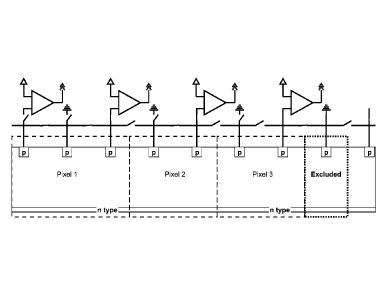
[0036] Figure 4a shows the conventional correction of misalignment. The
correction of
misalignment shown in Fig. 4a is that described in US Patent No. 8,300,276.
[0037] Figure 4b illustrates the correction of misalignment using one
embodiment of the
present teachings. In the embodiment shown in Fig. 4b, the boundaries (edges)
of the
detector pixels are changed from row to row in order to track the cross scan
movement of
the image elements as they are scanned across the detector array. Applying the
method of
these teachings, the cross scan misalignment (also referred to as cross scan
smear) can be
reduced to less than half a pixel. The reduction in misalignment results in
images with
better modulation transfer function. In applications, the reduction in
misalignment results
in reduced jitter requirements or reduce transmitted disturbance requirements
for the
system as a whole, or for pertinent subsystems.
[0038] In one instance, the embodiment of the method of these teachings
for correcting
misalignment also includes performing the following for each signal to yield a
plurality
of portions of a resulting image: obtaining the scan data from the each
signal, each signal
accumulating scan data of a portion of the target object; and generating image
data from
the scan data for a portion of the resulting image that corresponds to the
portion of the
target object.
Date recu/Date Received 2020/07/07
CA 02979035 2017-09-07
WO 2016/182622
PCT/US2016/021309
11
[0039] In another instance, the number of sub-columns per column is n, and
there
is misalignment at each segment if a portion of the target object has moved
substantially at least 1/2n of a column relative to the each column.
[0040] In one instance, each segment includes two or more rows of the
detectors.
[0041] In one or more other embodiments, the method of these teachings for
improving image resolution includes (a) receiving, at a detector array,
electromagnetic (EM) radiation from a target object. The detector array
includes
one or more detectors, the detectors organized into a plurality of segments,
each
segment having one or more rows of the detectors substantially perpendicular
to a
designed scan axis, each segment having one or more columns of detecting
components substantially parallel to the designed scan axis, each column
having
one or more sub-columns. The detector array moves in a relative scan direction
relative to the target object. A readout integrated circuit is operatively
connected
to the detector array, the readout integrated circuit including a number of
detector
boundary selection components, each one of the number of detector boundary
selection components configured to select or adjust a detector boundary at a
predetermined sub-column boundary or an adjustable sub-column boundary.
(b) The following are performed for each segment of the detector array. if
electromagnetic (EM) radiation is received from the target object in a first
detection, use detector boundaries in a conventional configuration, otherwise,
activate selected ones of the number of detector boundary selection
components.
(c) From each segment of the detector array, a plurality of signals is
obtained.
Steps (a) through (c) are repeated a predetermined number of times. The
selected
ones of the number of detector boundary selection components are selected to
produce a predetermined number of overlapping pluralities of signals. The
selected ones of the number of detector boundary selection components are also
selected according to an image resolution improvement prescription and/or
algorithm.
CA 02979035 2017-09-07
WO 2016/182622
PCT/US2016/021309
12
[0042] In one instance, each detector boundary selection component from the
number of detector boundary selection components is a switch. In another
instance, each detector boundary selection component from the number of
detector boundary selection components comprises at least two field
manipulators
(grids and/or implants) operatively attached to the detector array.
[0043] In one instance, detector (pixel) boundaries are moved by one of
right
shifting or left shifting and detector (pixel) size is substantially
preserved. In
another instance, detector (pixel) boundaries are moved and detector (pixel)
size
is not required to be constant.
[0044] Figure 5 shows one embodiment of the method of these teachings for
improving image resolution. Referring to Figure 5, in the embodiment shown
therein, in the first detection, the conventional pixel positions are used. In
the
subsequent detections, the detector boundary selection components are
activated
in order to obtain pixel positions such that the group of pixels is offset
from the
previous detection. Although in Figure 5, the pixels are shown as being all of
one
size, this embodiment is not limited to instances where the pixel size is
required to
be substantially constant.
[0045] The following is a disclosure by way of example of a device
configured to
execute functions (hereinafter referred to as computing device) which may be
used with the presently disclosed subject matter. The description of the
various
components of a computing device is not intended to represent any particular
architecture or manner of interconnecting the components Other systems that
have fewer or more components may also be used with the disclosed subject
matter. A communication device may constitute a form of a computing device and
may at least include a computing device. The computing device may include an
interconnect (e.g., bus and system core logic), which can interconnect such
components of a computing device to a data processing device, such as a
processor(s) or microprocessor(s), or other form of partly or completely
programmable or pre-programmed device, e.g., hard wired and or application
CA 02979035 2017-09-07
WO 2016/182622
PCT/US2016/021309
13
specific integrated circuit (ASIC), customized logic circuitry, such as a
controller
or microcontroller, a digital signal processor, or any other form of device
that can
fetch instructions, operate on pre-loaded/pre-programmed instructions, and/or
follow instructions found in hard-wired or customized circuitry to carry out
logic
operations that, together, perform steps of and whole processes and
functionalities
as described in the present disclosure.
[0046] In this description, various functions, functionalities and/or
operations
may be described as being performed by or caused by software program code to
simplify description. However, those skilled in the art will recognize what is
meant by such expressions is that the functions result from execution of the
program code/instructions by a computing device as described above, e.g.,
including a processor, such as a microprocessor, microcontroller, logic
circuit or
the like. Alternatively, or in combination, the functions and operations can
be
implemented using special purpose circuitry, with or without software
instructions, such as using ASIC or Field-Programmable Gate Array (FPGA),
which may be programmable, partly programmable or hard-wired. The ASIC
logic may be such as gate arrays or standard cells, or the like, implementing
customized logic by metalization(s) interconnects of the base gate array ASIC
architecture or selecting and providing metalization(s) interconnects between
standard cell functional blocks included in a manufacturer's library of
functional
blocks, etc. Embodiments can thus be implemented using hard-wired circuitry
without program software code/instructions, or in combination with circuitry
using programmed software code/instructions.
[0047] Thus, the techniques are limited neither to any specific combination
of
hardware circuitry and software, nor to any particular tangible source for the
instructions executed by the data processor(s) within the computing device.
While
some embodiments can be implemented in fully functioning computers and
computer systems, various embodiments are capable of being distributed as a
computing device including, e.g., a variety of forms and capable of being
applied
regardless of the particular type of machine or tangible computer-readable
media
CA 02979035 2017-09-07
WO 2016/182622
PCT/US2016/021309
14
used to actually effect the performance of the functions and operations and/or
the
distribution of the performance of the functions, functionalities and/or
operations.
[0048] The interconnect may connect the data processing device to define
logic
circuitry including memory. The interconnect may be internal to the data
processing device, such as coupling a microprocessor to on-board cache memory
or external (to the microprocessor) memory such as main memory, or a disk
drive
external to the computing device, such as a remote memory, a disc farm or
other
mass storage device, etc. .
[0049] The memory may include any tangible computer-readable media, which
may include but are not limited to recordable and non-recordable type media
such
as volatile and non-volatile memory devices, such as volatile RAM (Random
Access Memory), typically implemented as dynamic RAM (DRAM) which
requires power continually in order to refresh or maintain the data in the
memory,
and non-volatile ROM (Read Only Memory), and other types of non-volatile
memory, such as a hard drive, flash memory, detachable memory stick, etc. Non-
volatile memory typically may include a magnetic hard drive, a magnetic
optical
drive, or an optical drive (e.g., a DVD RAM, a CD ROM, a DVD or a CD), or
other type of memory system which maintains data even after power is removed
from the system.
[0050] At least some aspects of the disclosed subject matter can be
embodied, at
least in part, utilizing programmed software code/instructions. That is, the
functions, functionalities and/or operations techniques may be carried out in
a
computing device or other data processing system in response to its processor,
such as a microprocessor, executing sequences of instructions contained in a
memory, such as ROM, volatile RAM, non-volatile memory, cache or a remote
storage device. In general, the routines executed to implement the embodiments
of the disclosed subject matter may be implemented as part of an operating
system or a specific application, component, program, object, module or
sequence
of instructions usually referred to as "computer programs," or "software." The
computer programs typically comprise instructions stored at various times in
various tangible memory and storage devices in a computing device, such as in
CA 02979035 2017-09-07
WO 2016/182622
PCT/US2016/021309
cache memory, main memory, internal or external disk drives, and other remote
storage devices, such as a disc farm, and when read and executed by a
processor(s) in the computing device, cause the computing device to perform a
method(s), e.g., process and operation steps to execute an element(s) as part
of
some aspect(s) of the method(s) of the disclosed subject matter.
[0051] A tangible machine readable medium can be used to store software and
data that, when executed by a computing device, causes the computing device to
perform a method(s) as may be recited in one or more accompanying claims
defining the disclosed subject matter. The tangible machine readable medium
may
include storage of the executable software program code/instructions and data
in
various tangible locations, including for example ROM, volatile RAM, non-
volatile memory and/or cache. Portions of this program software
code/instructions
and/or data may be stored in any one of these storage devices. Further, the
program software code/instructions can be obtained from remote storage,
including, e.g., through centralized servers or peer-to-peer networks and the
like.
Different portions of the software program code/instructions and data can be
obtained at different times and in different communication sessions or in a
same
communication session.
[0052] The software program code/instructions and data can be obtained in
their
entirety prior to the execution of a respective software application by the
computing device. Alternatively, portions of the software program
code/instructions and data can be obtained dynamically, e.g., just in time,
when
needed for execution. Alternatively, some combination of these ways of
obtaining
the software program code/instructions and data may occur, e.g., for different
applications, components, programs, objects, modules, routines or other
sequences of instructions or organization of sequences of instructions, by way
of
example. Thus, it is not required that the data and instructions be on a
single
machine readable medium in entirety at any particular instance of time.
[0053] In general, a tangible machine readable medium includes any
tangible
mechanism that provides (i.e., stores) information in a form accessible by a
machine (i.e., a computing device, which may be included, e.g., in a
communication device, a network device, a personal digital assistant, a mobile
communication device, whether or not able to download and run applications
from the communication network, such as the Internet, e.g., an iPhone,
Blackberry, Droid or the like, a manufacturing tool, or any other device
including
a computing device, comprising one or more data processors, etc.
[0054] For the purposes of describing and defining the present
teachings, it is
noted that the term "substantially" is utilized herein to represent the
inherent
degree of uncertainty that may be attributed to any quantitative comparison,
value, measurement, or other representation.
The term "substantially" is also utilized herein to represent the degree by
which a
quantitative representation may vary from a stated reference without resulting
in a change
in the basic function of the subject matter at issue.
[0055] Although the invention has been described with respect to
various
embodiments, it should be realized these teachings are also capable of a wide
variety of further and other embodiments within the spirit and scope of the
appended claims.
16
Date Recue/Date Received 2021-01-06