Note : Les descriptions sont présentées dans la langue officielle dans laquelle elles ont été soumises.
WO 2017/081508 PCT/IB2015/002668
1
Process for manufacturing a non-opaque layer for a multilayer structure
comprising a window, and a multilayer with such a non-opaque layer.
[cm ] The invention relates to improvements in the domain of processes for
manufacturing multilayer structures comprising a non-opaque window. Such a non-
opaque window, which may be transparent, is used for instance in security
documents or cards having laminate structures, for increasing the difficulty
to
counterfeit and forge them.
[002] Figure 1 shows a multilayer structure used in the course of a prior
art
manufacturing process of this type. It comprises
- a transparent substrate 1 including a thermoplastic material,
- compensation layers 2 with a window 3 and
- transparent patches 4 positioned in the windows 3 over the transparent
substrate 1.
[003] Other layers 5 may be stacked up on one or both sides of such a
structure,
before lamination. Patent application n WO 2013/038361 discloses same or
similar
multilayer structures.
[004] The manufacturing process of such a structure requires a precise
alignment
of the various layers which add some complexity to this kind of manufacturing
process. Moreover, these complex additional process steps increase
manufacturing
time and costs.
[005] Another manufacturing process is disclosed in patent application n
WO
2014/203199A1. In this process, layers having a window are laminated with a
transparent layer made of thermoplastic material. Both the layers having a
window
and the transparent layer will be part of the final multilayer structure as it
will be used.
But, such a multilayer structure obtained with such a process may have
defaults and
deformations.
[006] An aim of the invention consists in simplifying and/or improving
manufacturing
processes of this type.
[007] This aim
is at least partly achieved with a process for
manufacturing a non-opaque layer to be included in a multilayer structure
comprising
at least one non-opaque window. Indeed, thanks to the process of claim 1, a
non-
opaque layer is made with a region having an extra-thickness which is more
easily
Date Recue/Date Received 2021-10-12
WO 2017/081508 PCT/IB2015/002668
2
inserted and aligned with the window or cu-out made in an adjacent layer. The
region
with the extra-thickness may sufficiently fill this window or cut-out for
avoiding the use
of patches in the window. Further, the patterned plate which is heated for
making the
non-opaque material flowing in its cavity, is removed and is not part of the
final
structure. The material of the patterned plate can be specifically chosen for
its
function, i.e. forming a cavity within which the non-opaque material can flow
for
shaping the region with the extra-thickness.
[0os] Further features and/or advantages of the manufacturing process
are presented.
[009] According to another aspect, the invention is a process
for manufacturing a multilayer structure comprising a non-opaque
layer.
[001 0] According to another aspect, the invention is semi-finished product
.
[0011] According to another aspect, the invention is a multilayer structure
.
[0012] According to another aspect, the invention is a security article .
[0013] Other features and advantages of the invention will be apparent from
the
following description and from an inspection of the accompanying drawings in
which:
[0014] - Figure 1 is a schematic cross section of a stack up of layers to
be used in a
prior art process;
[0015] - Figure 2 Is a schematic front view of an example of a card with a
clear
window, manufactured according to the invention;
[0016] - Figure 3 is a schematic cross section of a non-opaque layer
inserted
between patterned and covering sheets, before lamination;
[0017] - Figure 4 is a schematic cross section of the non-opaque layer of
Figure 3,
with a region having an extra-thickness resulting from the lamination;
[0018] - Figure 5 is a schematic cross section of a non-opaque layer with a
region
having an extra-thickness, laminated with compensation and finishing layers,
in a
finished card;
Date Recue/Date Received 2021-10-12
CA 03005002 2018-05-10
WO 2017/081508 PCT/IB2015/002668
3
[0019] - Figure 6 is schematic cross section, similar to the one of figure
5, of a
multilayer structure obtained according to another embodiment of the inventive
process ; and
[0020] - Figure 7 is schematic cross section, similar to the one of figure
5 or 6, of a
multilayer structure obtained according to another embodiment of the inventive
process.
[0021] On the drawings, same reference numerals denote the same elements.
[0022] The invention is hereafter explained with reference to identity card
applications. However, it is to be understood that the invention can be
implemented
for other applications such as smartcards, passports, badges, etc., and in
particular,
when a see-through portion or window is required.
[0023] Figure 2 shows a card 10 with a see-through window 11 (which may be
a
clear or transparent window, or more generally a non-opaque window).
[0024] An example of process according to the invention is described with
reference
to Figures 3 to 5. According to this example, an insert or inlay is achieved
in the first
place. As illustrated on figure 3, for obtaining a card 10, the manufacturing
process
comprises embossing a middle layer or inlay. Consequently, a non-opaque layer
12 is
provided. Such a non-opaque layer 12 is made of non-opaque plastic material
including but not limited to one of the following compounds: polycarbonate
(PC),
poly(vinyl-chloride) (PVC), polyethylene terephthalate (PET), polyethylene
terephthalate glycol modified (PETg), polyethylene terephthalate film (PETf),
polylactic acid (PLA), polyethylene (PE) or polyestercarbonate (PEC). The non-
opaque layer 12 can be a stack up of different layers. The initial thickness
of the non-
opaque layer 12 (before embossing and lamination) is for example in the range
of 100
pm up to 650 m.
[0025] The layer 12 of non-opaque material is then placed between patterned
plates,
sheets or layers 14. The material of these patterned plates (or covering them)
is
chosen for example in order not to stick to the layer 12 of non-opaque
material, after
its embossing. Openings are made in such patterned plates for example by
punching.
Covering sheets or plates 18 are placed so as to cover respectively each
patterned
plate 14 and its opening(s). Cavities 16 are then obtained. Each cavity 16
opens
toward the respective main surface of the layer 12 of non-opaque material. The
material used for forming the patterned plates 14 and covering sheets 18 is
included
CA 03005002 2018-05-10
WO 2017/081508 PCT/IB2015/002668
4
in, but not limited to, the list of following compounds: paper, metal and
liner plastic
film.
[0026] As show on Figure 4, this stack of layer 12, plates 14 and sheets 18
is then
laminated between lamination plates 26, for embossing the layer 12 of non-
opaque
material. This first lamination process comprises a hot pressing cycle
followed by a
cool cycle. For example, when the non-opaque material is polycarbonate, during
the
hot pressing cycle, the non-opaque material is pressed with a temperature in a
range
from 160 C to 195 C and a pressure in a range from 17 to 110 N/cm2, for a
duration
between 15 and 45 mn. More generally, for other materials than polycarbonate,
during the hot pressing cycle, the non-opaque material may be pressed with a
temperature in a range from 120 C to 195 C and a pressure in a range from 17
to
110 N/cm2, for a duration between 15 and 45 mn. After the hot pressing cycle,
the
non-opaque material has flowed in the cavities 16. For example, when the non-
opaque material is polycarbonate, during the cool pressing cycle, the stack of
layers
12, 14, 18 is pressed with a temperature in a range from 15 C to 25 C and a
pressure
in a range from 50 to 220 N/cm2, for a duration between 13 and 45 mn. The cool
cycle
allows "freezing" the layer 12 of non-opaque material and limits its
shrinking.
[0027] Alternatively, according to an embodiment which is not illustrated,
the
openings 16 are not punched over the whole thickness of the patterned plates
14. In
this case, cavities or hollows 16 are rather etched or milled over a part of
the
patterned plate thickness. Covering sheets 18 and/or lamination plates 26
become
then optional. In other words, they are all part of the patterned plates 14.
The
patterned plates are then positioned over the layer of non-opaque material so
that
each cavity opens toward the respective main surface of the layer of non-
opaque
material.
[0028] After the hot pressing cycle, the non-opaque material has flowed in
the
cavities 16. The final thickness of the layer 12 of non-opaque material, in a
first region
13, wherein the layer 12 of non-opaque material is thinner, is close to the
initial
thickness of layer 12 before lamination (i.e. within a range of 0 to 20 pm
thinner). The
final thickness of the layer 12 of non-opaque material, in a second region 15,
wherein
the layer 12 of non-opaque material is the thickest, is 10 to 80 % thicker
than the
thickness of the first region 13. The layer 12 of non-opaque material
consequently has
CA 03005002 2018-05-10
WO 2017/081508 PCT/IB2015/002668
an extra-thickness (in the second region 15 compared to the first region 13),
which
substantially corresponds to the depth of the cavities 16.
[0029] After this first lamination process, the patterned plates 14 and
covering 18
sheets are separated and removed from the layer 12 of non-opaque material.
Both
5 main surfaces of the layer 12 of non-opaque material are then free.
Possibly, the
material of the patterned plates 14 and covering 18 sheets is such that these
main
surfaces of the layer 12 of non-opaque material have a controlled roughness
for
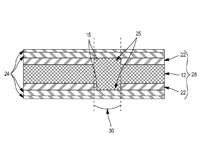
improving the cohesion with further layers.
[0030] The layer 12 of non-opaque material with its extra-thickness regions
15 is
subsequently prepared for a second lamination process, for making the final
card
structure shown on Figure 5.
[0031] Compensation 22 and finishing 24 layers are laid over the layer 12
of non-
opaque material (the compensation layers 22 first laid over the layer 12 of
non-
opaque material and then the finishing layers 24 respectively laid over each
compensation layer 22). The function of a compensation layer 22 is to
compensate
the extra-thickness of the layer 12, so as to have a substantially flat
surface over
which the finishing layer 24 with lay. The compensation layers 22 and
finishing layers
24 are for example made of plastic materials which are compatible with the
material
used for layer 12. For example, if the layer 12 is in polycarbonate material,
the
compensation layers 22 and finishing layers 24 may be in polycarbonate
material too,
within the needed thickness in order to reach the final targeted card
thickness. For
example, the layer 12 is transparent and 340 m thick in the first region 13,
the
compensation layers 22 are white and 100 m thick and the finishing layers 24
are
transparent and each made of two layers, respectively 50 and 100 m thick (as
show
on figure 7 which will be described below with more details).
[0032] Each compensation layer 22 has a window 25 in coincidence with the
second
region 15 (i.e. the region of the layer 12 of non-opaque material having an
extra-
thickness). It is easy to align the second regions 15 of the layer 12 of non-
opaque
material and the windows 25, therefore simplifying and rendering more
efficient the
manufacturing process. Indeed, the extra-thickness of the second regions 15
the layer
12 of non-opaque material can be used for abutting the edges of the windows
25. In
other words, the window 25 is filled in by the second region 15 the layer 12
of non-
opaque material. Even, if due to tolerances, it remains a small gap between
the edges
CA 03005002 2018-05-10
WO 2017/081508 PCT/IB2015/002668
6
of second region 25 and those of the windows 25, it will not have any
consequence
since during a second lamination process, the possible gap will be filled (the
non-
opaque material and/or the material of the compensation layers 22 will flow or
creep
into this gap).
[0033] After the
second lamination process, this stack of layers 12, 22, 24 forms a
multilayer structure (or laminate) 28. Of course only layers 12 and 22 can
form a
multilayer structure which can be sufficient for other applications or
purposes.
[0034] With the above-described manufacturing process, several cards 10 are
then
manufacturing at once and cut out in the multilayer structure 28 to make final
cards.
This manufacturing process allows making several multilayers structures with
precise
alignment within a repeatable, efficient and costs effective process.
[0035] According
this invention the alignment of non-opaque plastic material within
the window is accurate and the application of a security feature bigger than
the
window will not be deformed whereas in the case of the patch in the prior art,
the non
accurate alignment will induce a deformation of the security feature at the
boundary of
the window.
[0036] According to another embodiment shown on figure 6, the layer of non-
opaque
material is made of two layers 12a and 12b of the same non-opaque material.
Originally, these layers 12a and 12b of non-opaque material are separate.
Then,
before the step above-described with regard to figure 3, an antenna 40 (the
dots on
Fig. 6 represent the cross-section of the antenna loops) and a chip 50 are
inserted
between layers 12a and 12b of non-opaque material. The next steps of the
process
are similar to the ones above-described. The dotted line 12c between layers
12a and
12b only virtually separate layers 12a and 12b, but of course has no physical
materiality after the lamination step resulting in a single layer of non-
opaque material
with its extra-thickness region 15.
[0037] Another
embodiment of the inventive process is shown on figure 7. On this
figure, the layer 12 of non-opaque material is inserted between compensation
layers
22 and finishing layers 24. For this illustrated example, a security element
51 is
inserted between two finishing layers 24 covering the same side of the
multilayer
structure 28. This security element 51 can have a shape with dimensions larger
or
smaller than the corresponding ones of the window 30. A security background 52
can
also be applied on a layer or inserted between two layers of the multilayer
structure
CA 03005002 2018-05-10
WO 2017/081508 PCT/IB2015/002668
7
28. For this illustrated example, security backgrounds 52 are applied on a
finishing
layer 24, facing a compensation layer 22, on each side of the multilayer
structure 28.
For example, in the illustrated multilayer structure 28, the layer 12 is
transparent and
340 m thick in the first region 13, the compensation layers 22 are white and
100 m
thick and the finishing layers 24 are transparent and each made of two layers,
respectively 50 and 100 m thick (the thinner being internal).
[0038] Many variations of the above-described processes can be envisioned.
For
examples
[0039] - see-through windows 30 corresponding to the second regions 15 on each
side of the multilayer structure 28 can have different shapes and/or sizes;
[0040] - the non-opaque plastic material of layer 12 can be mass-colored.
[0041] The layer 12 and/or the multilayer structure 28 can be used for many
applications, for example:
[0042] - according to one application, the layer 12 does not contain any
smart
component, in this case data can be stored in magnetic strips inserted between
finishing layers (as the security background 52, shown on figure 7);
[0043] - according to another application, the layer 12 is inserted in a
multilayer
structure 28 which will be milled in an area different from the window 30, for
attaching
a chip module with terminals for contact communication with a card reader;
[0044] - according to another application, an antenna and a chip are
inserted in the
layer 12 as already described with regard to figure 6, for making a
contactless card;
[0045] - according to another application, an antenna is inserted between
two
layers constituting the layer 12, prior to laminate it in a multilayer
structure and milling
a cavity within which a chip module with terminals will be attached and
connected to
the antenna for making a dual interface card;
[0046] - according to another application, an antenna and a chip are
inserted in the
layer 12 as already described with regard to figure 6, and a cavity is milled
in the
multilayer structure 28, for accommodating a chip module with terminals and
achieving an hybrid card.