Note : Les descriptions sont présentées dans la langue officielle dans laquelle elles ont été soumises.
1
TITLE
[0001] A
method of providing power input to a flexible printed circuit and a flexible
printed circuit having power input in accordance with the method.
FIELD
[0002] There
is described a method of providing power input to a flexible printed circuit
and a flexible printed circuit having power input in accordance with the
method.
BACKGROUND
[0003]
International Patent Publication W02017/127943 (Carel) titled "Flexible
Printed
Circuit" describes that Point of Purchase (POP) stand-up displays are
typically constructed
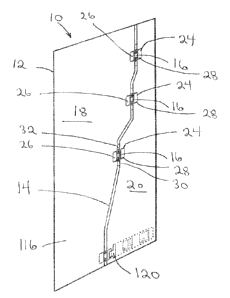
by cutting a small hole out through cardboard that has been imprinted with
graphics. An
LED is then manually pushed through the hole, so the LED protrudes from a
front of the
cardboard and is secured in place with tape positioned at a back of the
cardboard. A
conductive wire extends to a power transformer box, which is attached to the
back of the
cardboard by double sided adhesive tape. A power cord is run from the power
transformer
box to an external power outlet in a wall. When activated, the LED blinks on
and off.
[0004] The
Carel reference goes on to describe a flexible printed circuit that can be
rolled or folded. The Carel reference further describes "butterfly" connectors
that are used to
connect electrical components, such as light emitting diodes (LEDs), to the
flexible printed
circuit. The connectors are referred to as "butterfly" connectors due to their
shape, having a
body with a central portion and opposed wing portions.
[0005] To integrate
large numbers of LEDs into a thin flexible circuit, with the ability to
control each LED separately, it is necessary to provide at least one control
line per LED with
common power (direct control), or two individual control lines (some can be
shared in
multiplexed scenarios). Routing these large number of traces can be a
difficult task, and as
density increases, the trace width must decrease to accommodate. This
necessitates a thicker
conductive material, to ensure adequate power delivery, compromising the
flexibility of the
circuit and increasing the cost. In addition, it is often necessary to have
traces cross and,
CA 3016051 2018-08-31
2
therefore, multiple layers are needed.
[0006] There
will hereinafter be provided an alternative approach to providing power to
electrical components on a flexible printed circuit.
SUMMARY
[0007]
According to one aspect there is provided a method of providing power input to
a
flexible printed circuit. The method involves the step of bisecting a flexible
printed circuit
into a first conductive area adapted for power input and a second conductive
area adapted for
ground connection. In accordance with this teaching, power input is provided
to electrical
components attached to the flexible printed circuit via first conductive area
and second
conductive area.
[0008] It
will immediately be apparent that the above described method does not restrict
flexibility to the degree that the use of control lines unavoidably does.
[0009] There
will hereinafter be described the use of this method in a practical
application. In the
described application the flexible printed circuit is bisected by
communication lines between the electrical components. The electrical
components are light
emitting diodes (LEDs), which are attached to the flexible printed circuit by
a conductive
adhesive. It is preferred that the LEDs have integrated controllers that use a
serial
communications protocol that facilitates daisy chaining. It will be understood
that LEDs
have been chosen as the most obvious immediate application for the method.
However, the
method has broader application to other electrical components.
[0010]
According to another aspect, there is provided a flexible printed circuit that
has
been fabricated in accordance with the method. The flexible printed circuit
has a flexible
printed circuit substrate bisected by communication lines between electrical
components into
a first conductive area adapted for power input and a second conductive area
adapted for
ground connection. Electrical
components are attached to the substrate along the
communication lines and connected to the first conductive area and the second
conductive
CA 3016051 2018-08-31
3
area. With this connection power input is provided to the electrical
components via first
conductive area and second conductive area.
BRIEF DESCRIPTION OF THE DRAWINGS
[0011] These and other features will become more apparent from the
following
description in which reference is made to the appended drawings, the drawings
are for the
purpose of illustration only and are not intended to be in any way limiting,
wherein:
[0012] FIG. 1 is a rear elevation view of a flexible conductive circuit
developed for use
with a display.
[0013] FIG. 2 is a front elevation view of a display into which has been
incorporated the
flexible conductive circuit of FIG. 1.
[0014] FIG. 3 is an exploded side elevation view of the display of FIG.
2.
[0015] FIG. 4 is a front elevation view of the flexible conductive
circuit of FIG. 1.
[0016] FIG. 5 is a rear elevation view of the display of FIG. 2.
DETAILED DESCRIPTION
[0017] A flexible printed circuit generally identified by reference
numeral 10, will now
be described with reference to FIG. 1. A display 100 will then be described
with reference to
FIG. 2 through FIG. 5.
Method
[0018] Referring to FIG. 1, in broad terms the method of providing power input
to flexible
printed circuit 10 consists of bisecting flexible printed circuit 10 into
first conductive area 18
adapted for power input and a second conductive area 20 adapted for ground
connection.
Power input is then provided to electrical components, such as LEDs 16,
attached to flexible
printed circuit 10 via first conductive area 18 and second conductive area 20,
rather than
through individual control lines.
Structure and Relationship of Parts:
[0019] Referring to FIG. 1, there will now be described the application of
the teachings of
the method to a practical application represented by flexible printed circuit
10. Flexible
CA 3016051 2018-08-31
4
printed circuit 10 has a flexible printed circuit substrate 12 bisected by
communication lines
14 between electrical components, in the form of light emitting diodes 16
(LEDs) into a first
conductive area 18 adapted for power input and a second conductive area 20
adapted for
ground connection. Light emitting diodes 16 (LEDs) are attached to substrate
12 along
communication lines 14. Butterfly connectors 24 are used to mount LEDs 16.
Each
butterfly connector 24 has a first wing 26 and a second wing 28. A conductive
adhesive (not
visible in this view) is used to attach each butterfly connector 24 to
substrate 12, with first
wing 26 connected to first conductive area 18 and second wing 28 connected to
second
conductive area 28. As will hereinafter be described in relation to method and
operation,
power input is provided to LEDs 16 via first conductive area 26 and second
conductive area
28.
[0020] It is preferred that LEDs 16 have integrated controllers that use
a serial
communications protocol that facilitates daisy chaining. Such a system can be
implemented
by using serially addressable LEDs such as the ws2812. These red, green blue
(RGB) LEDs
integrate a serial shift register utilizing either a 1 wire or 2 wire serial
communication
interface. Thus, large common traces can be used to deliver power (voltage and
ground),
while thin traces connecting the LEDs in sequence provide the signals needed
to control the
color and brightness of each LED. Common flood filled power delivery areas can
be used as
well, reducing the amount of material that needs to be removed for subtractive
fabrication
methods. This also dramatically simplifies the design of the circuit, as
individual traces from
the controller to each LED are no longer needed.
[0021] Each addressable LED 16 receives power through integrated contacts
on it's
breakout board which connect to of power delivery regions of first conductive
area 26 and
second conductive area 28. Input signal data comes from input contact 30
through serial
communication line 14, from either the controller output or the output of the
previous LED
in the linear daisy chain, which signal is output to the next LED through
output contact 32,
again through serial communication line 14.
Cautionary Warnings:
CA 3016051 2018-08-31
5
[0022] It is recommended that an Electrostatic Discharge (ESD)
mitigation component
be used to protect electrical components on the flexible printed circuit from
damages due to
static electrical discharge during handling. ESC mitigation components can be
integrated
into electrical components, such as the controllers of LEDs 16.
Incorporation of flexible circuit 10 into display 100
[0023] Referring to FIG. 2, there is illustrated a front elevation view
of display 100 into
which flexible conductive circuit has been incorporated. Display 100 includes
a graphic
overlay 102. Graphic overlay 102 has an alpha-numeric message 104. The
messages
chosen for illustration is "Look Here For Todays Big Savings" In order to draw
attention of
the public to graphic overlay 102 and alpha-numeric message 104, display 100
has
"windows" for display elements to show through. Two different sizes of
"windows" have
been selected for illustration: a series of three small windows 106 and a
single larger window
108.
[0024] Referring to FIG. 3, there is illustrated an exploded side
elevation view of the
various layers that make up display 100. Those layers include graphic overlay
102, flexible
conductive circuit 10 and a conformal protective backing layer 110. Also
visible in this view
are butterfly connectors 24 supporting LEDs 16. As previously described,
butterfly
connectors 24 secure LEDs to flexible conductive circuit 10. As will
hereinafter be further
described, LEDs 16 are positioned so that they light they project is visible
through small
windows 106 of graphic overlay 102. Also visible in this view is an ePaper
display element
112. As will hereafter further described ePaper display element 112. ePaper
display element
112 has been chosen for illustration, to demonstrate that various display
elements can be
used. The application is not restricted to the use of LEDs. As will
hereinafter be further
described, ePaper display element 112 is positioned so that the light it
projects is visible
through larger window 108 of graphic overlay 102. To assist in orientation,
flexible printed
circuit substrate 12 for flexible conductive circuit 10 is shown in FIG. 3, as
having a front
face 114 on which is positioned a front circuit and a rear face 116 on which
is positioned a
rear circuit.
CA 3016051 2018-08-31
6
[0025] This
example has been selected to demonstrate that a circuit need not be limited
to one face of substrate 12. There can be a rear circuit on a rear face 116
and a front circuit
on a front face 114. Referring to FIG. 4, there is illustrated a front
elevation view showing
front face 114 of flexible conductive circuit 10. From this front elevation
view, it can be
seen that flexible conductive circuit 10 has three small windows 106, which
correspond to
the three small windows 106 in graphic overlay 102. The small windows 106 have
been
given the same reference numeral to help the reader understand that they are
aligned so that
LEDs 16 mounted to rear face of flexible conductive circuit 10 are visible
through small
windows 106 on graphic overlay 102. Also visible is a connector circuit 118
for ePaper
display element 112. Connector circuit 118 is connected to controller 120 on
rear face 116 of
flexible conductive circuit 10, with a flexible connector that extends through
holes in
substrate 12 for flexible conductive circuit 10 or wraps around an edge of
substrate 12.
[0026]
Referring to FIG. 5, rear face 116 of flexible conductive circuit is protected
by
conformal protective backing layer 110. Backing layer 110 is secured by rear
face 116 of
flexible conductive circuit 10 by adhesive arranged in a pattern of dots 122.
[0027] In
this patent document, the word "comprising" is used in its non-limiting sense
to mean that items following the word are included, but items not specifically
mentioned are
not excluded. A reference to an element by the indefinite article "a" does not
exclude the
possibility that more than one of the element is present, unless the context
clearly requires
that there be one and only one of the elements.
[0028] The
scope of the claims should not be limited by the illustrated embodiments set
forth as examples, but should be given the broadest interpretation consistent
with a purposive
construction of the claims in view of the description as a whole.
CA 3016051 2018-08-31