Note : Les descriptions sont présentées dans la langue officielle dans laquelle elles ont été soumises.
DESCRIPTION
OPTICAL MODULE
Technical Field
[0001] The present invention relates to an optical module including a Si
photonic lightwave
circuit connectable to an optical fiber.
Background Art
[0002] Development of optical modules using silicon (Si) photonic elements
such as, for
example, an optical modulator, an optical receiver, and a coherent optical sub-
assembly (COSA)
obtained by combing the optical modulator and the optical receiver is now
popular. The Si
photonic element is formed of a lightwave circuit in which fine optical
waveguides are formed,
the optical waveguides using, as a core material, silicon which is widely used
as a
semiconductor and which has a far greater refractive index than silicon oxide
films and
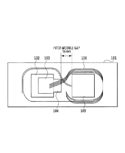
polymers. The optical waveguide using the Si core has a relative refractive
index ten times or
more than that of a conventional PLC, a mode field diameter (MFD) 1/10 or less
thereby
achieving strong confinement in a micron order, and a small minimum bend
radius (5 pm or
less). Accordingly, the Si photonic element has a characteristic of being far
smaller than the
conventional optical device, and an optical module such as an optical
transceiver which has a
smaller size and a higher density packaging than the conventional optical
device is expected to
be achieved.
[0003] This Si photonic element and small optical parts are usually used in
combination with
other optical fiber pigtail modules such as an LD module. There is a demand
for size reduction
not only for each of these modules but also for an entire sub-board for
connecting the modules
with optical fibers and packaging them in combination or an entire case for
housing the modules
such as, for example, a case with size restriction such as CFP2.
[0004] The Si cores of the optical waveguides in the Si photonic element are
finer than cores
formed by using a silicon dioxide (SiO2) film and are formed in a square each
side of which is in
sub-micron order. When such fine optical waveguides are simply connected to
normal optical
fibers, the optical
- 1 -
CA 3023857 2020-03-30
CA 03023857 2018-11-09
coupling loss is large. Accordingly, the mode field diameter of light emitted
from an end of
each optical waveguide needs to be increased.
[0005] Specifically, in the Si photonic lightwave circuit, optical waveguides
are integrated with
the radius of curvature being about 5 i_tm, and the functions of the circuit
are achieved in a
smaller space. In addition, more and more optical fibers and electric circuits
are employing
multi-array designs. However, the radius of curvature of the optical fibers is
about, for example,
15 mm. Accordingly, it is necessary to reduce not only the size of the Si
photonic lightwave
circuit but also the size of a module group including routed portions of
external optical fibers.
[0006] Fig. 11 illustrates a typical example of a conventional Si photonic
element. Two
package modules 1102, 1105 are mounted on the same board 1101. In this
example, a Si
photonic lightwave circuit 1103 is 20 mm square and is mounted on the 30 mm
square package
module 1102. Moreover, the Si photonic lightwave circuit 1103 is connected to
an optical fiber
array 1106 fixed by an optical fiber two-core ferrule (8x10 mm) 1104 which is
fixed on a right
side of the Si photonic lightwave circuit 1103 in the drawing. Methods of
connecting a
two-core optical waveguide of the Si photonic lightwave circuit 1103 to the
optical fiber array
1106 include a method of fixing the optical fiber ferrule with YAG welding
while interposing a
lens, a method of fixing the metal-coated optical fiber with solder, and the
like.
Citation List
Non Patent Literature
[0007] NPL 1: Jaime Cardenas, "High Coupling Efficiency Etched Facet Tapers in
Silicon
Waveguides," IEEE Photon. Lett., Vol.26, p.2380, 2014.
Summary of Invention
Technical Problem
[0008] The optical waveguide of the Si photonic lightwave circuit 1103 is
perpendicular to a
right side edge of the Si photonic lightwave circuit 1103 and the optical
fiber array 1106 is also
connected perpendicularly to the right side edge. Accordingly, the optical
fiber array 1106
would come into contact with the right optical module 1105. Moreover, a space
for routing the
optical fibers cannot be generally provided in a direction perpendicular to
the substrate surfaces
- 2 -
of the package modules 1102, 1105 due to heat dissipation and the like, and
the package modules
and the optical fibers cannot be laid one over the other. Accordingly, in
order to route the optical
fibers around the package module 1105 as in Fig. 11, the package modules 1102,
1105 needs to be
arranged to be spaced away from each other by a certain distance in
consideration of the radius of
curvature of the optical fibers which is 15 mm. In one example of the
arrangement, an interval
of 27 mm or more needs to be provided between the package modules 1102, 1105.
[0009] As described above, the conventional design has a problem that, when
the optical fibers
are connected to the module including the Si photonic lightwave circuit, the
interval between the
modules is as large as the size of the modules and the modules cannot be
arranged in a small space.
[0010] The present invention has been made in view of the problems described
above and an
object thereof is to provide an optical module which is connectable to an
optical fiber array and
which can be packaged in a high density.
Solution to Problem
[0011] In order to solve the aforementioned problem, the present invention
provides an optical
module comprising: a Si photonic lightwave circuit including an optical
waveguide formed of a Si
core and a SiO2 cladding, the optical waveguide tilted on an output end
surface at an oblique angle
with respect to a direction perpendicular to the output end surface; and an
optical fiber block fixing
an optical fiber array at the same oblique angle as the optical waveguide,
wherein a center of the
optical waveguide on the output end surface is shifted from a center of a side
surface of the Si
photonic lightwave circuit including the output end surface in a direction to
which the optical
waveguide is tilted, and the optical fiber array is bended between a second
module and the optical
module on which the Si photonic lightwave circuit is mounted such that the
optical fiber array does
not overlap the second module, wherein the optical module and the second
module are mounted
on a board and arranged such that the second module faces the side surface
including the output
end surface.
[0012] In another aspect of the present invention, the output end surface of
the optical waveguide
in the Si photonic lightwave circuit is perpendicular to a mount surface of
the Si photonic lightwave
circuit.
- 3 -
Date Recue/Date Received 2020-11-19
[0013] In another aspect of the present invention, the optical waveguide in
the Si photonic
lightwave circuit is an optical waveguide array in which a plurality of
optical waveguides are
arranged parallel to each other.
-3a -
Date Recue/Date Received 2020-11-19
CA 03023857 2018-11-09
[0014] In another aspect of the present invention, the optical waveguide in
the Si photonic
lightwave circuit includes a spot size increasing portion formed of a tapered
portion in which a
width of the Si core decreases toward the output end surface.
[0015] In another aspect of the present invention, the oblique angle is 5
degrees or more and 50
degrees or less.
[0016] In another aspect of the present invention, the optical waveguide in
the Si photonic
lightwave circuit includes a waveguide with a constant width at a end point of
the tapered portion
in which the width of the Si core decreases toward the output end surface.
Advantageous Effects of Invention
[0017] In the present invention, an optical module which is connectable to an
optical fiber array
can be packaged in a high density.
Brief Description of Drawings
[0018]
[Fig. 1] Fig. 1 is a view illustrating a configuration of optical modules
according to
Embodiment 1 of the present invention;
[Fig. 2] Fig. 2 is a view illustrating a configuration of optical modules
according to
Embodiment 2 of the present invention;
[Fig. 3] Fig. 3 is a view illustrating a configuration in which two of the
configurations
illustrated in Fig. 2 are mounted on the same chassis 301;
[Fig. 4A] Fig. 4A is a view illustrating a connection portion between an
optical waveguide of a
Si photonic lightwave circuit and an optical fiber block;
[Fig. 4B] Fig. 4B is a view illustrating a module interval at each oblique
angle 0 in the case
where the minimum bent radius of an optical fiber is 15 mm;
[Fig. 5A] Fig. 5A is a view illustrating the connection portion between the
optical waveguide
of the Si photonic lightwave circuit and the optical fiber block;
[Fig. 5B] Fig. 5B is a view illustrating a module interval at each oblique
angle 0 in the case
where the minimum bent radius of the optical fiber is 5 mm;
- 4 -
CA 03023857 2018-11-09
[Fig. 6A] Fig. 6A is a view illustrating an enlarged view of an optical
waveguide array in the Si
photonic lightwave circuit;
[Fig. 6B1 Fig. 6B is a view illustrating a cross-sectional view of the optical
waveguide array in
the Si photonic lightwave circuit;
[Fig. 7A] Fig. 7A is a view illustrating a configuration of a spot size change
portion;
[Fig. 7131 Fig. 7B is a view illustrating the configuration of the spot size
change portion;
[Fig. 8A] Fig. 8A is a view illustrating a configuration of a spot size change
portion having a
structure with a constant width at a tapered front end;
[Fig. 8B1 Fig. 8B is a view illustrating the configuration of the spot size
change portion having
the structure with the constant width at the tapered front end;
[Fig. 9] Fig. 9 is a view illustrating dependence of a reflection loss on an
optical waveguide
angle in each of a Si optical waveguide which has a MFD of 1.0 pm and an
optical waveguide in
the Si photonic lightwave circuit which has a MFD of 5.0 lam;
[Fig. 10] Fig. 10 is a view illustrating an effect of reducing a coupling loss
by increasing the spot
size of the optical waveguide in the Si photonic lightwave circuit; and
[Fig. 11] Fig. 11 is a view illustrating a typical example of a conventional
Si photonic element.
Description of Embodiments
[0019] Embodiments of the present invention are described below in detail.
[0020] (Embodiment 1)
Fig. 1 illustrates a configuration of optical modules according to Embodiment
1 of the
present invention. In the embodiment, as in the configuration of Fig. 11, two
30 mm square
package modules 102, 105 are mounted on a board 101, and optical waveguides of
Si photonic
lightwave circuit 103 in a 20 mm square mounted on the package module 102 are
connected to
an optical fiber array 106 fixed to an optical fiber block (15x10 mm) 104.
Moreover, output
end surfaces of the optical waveguides in the Si photonic lightwave circuit
103 are perpendicular
to a mount surface of the package module 102 which is a surface on which the
board 101 and the
package module 102 are in contact with each other or to a mount surface of the
Si photonic
lightwave circuit 103 on which the package module 102 and the Si photonic
lightwave circuit
- 5 -
CA 03023857 2018-11-09
103 are in contact with each other. In this case, the position of a center
waveguide or the center
between optical waveguides at both ends on the end surface is set at the
center (point 15 mm
away from upper and lower ends) of the right side edge of the package module
102 which is the
output end surface, as in the configuration of Fig. 11 for comparison with the
conventional
example.
[0021] Meanwhile, in the embodiment, the optical waveguides in the Si photonic
lightwave
circuit 103 are tilted at an appropriate angle, for example, 20 degrees with
respect to a direction
perpendicular to the right end surface. Moreover, the optical fiber block 104
fixes optical fibers
with the optical fibers tilted at 20 degrees with respect to a direction
perpendicular to an end
surface connected to the Si photonic lightwave circuit 103.
[0022] As described later, the MFD of the optical waveguides in the Si
photonic lightwave
circuit 103 is increased at the end surface to be set to the same field
diameter as the optical fibers.
Accordingly, the optical waveguides in the Si photonic lightwave circuit 103
and the optical
fibers are tilted at the same angle with respect to the direction
perpendicular to the connection
end surface and can be connected to one another on the same straight lines.
Using the Si
photonic lightwave circuit 103 and the optical fiber block 104 as described
above can greatly
reduce the inter-package gap between the package modules 102, 105, which is 27
mm in the
conventional example illustrated in Fig. 11, to 16 mm and reduce the inter-
package gap to about
half the package module length which is 30 mm.
[0023] (Embodiment 2)
Fig. 2 illustrates a configuration of an optical module according to
Embodiment 2 of the
present invention. In the embodiment, as in Embodiment 1, two 30 mm square
package
modules 202, 205 are mounted on a chassis 201, and optical waveguides in a 20
mm square Si
photonic lightwave circuit 203 mounted on the package module 202 is connected
to an optical
fiber array 206 fixed to an optical fiber block (15 x10 mm) 204.
[0024] In Embodiment 2, the positions of the optical waveguides in the Si
photonic lightwave
circuit are shifted from a portion around the center of the package module to
the side to which
the optical waveguides are tilted (upper side in the drawing) to further
reduce the gap between
- 6 -
CA 03023857 2018-11-09
packages from that in the configuration of Embodiment 1. As illustrated in
Fig. 2, a center
optical waveguide in the Si photonic lightwave circuit 203 is shifted from the
center of the right
side edge which is an output end surface of the package module 202 to the
upper side of the
drawing by 5 mm, and the optical fiber block 204 is similarly shifted to the
upper side of the
drawing by 5 mm. This can reduce the gap between the package modules 202, 205
from 16
mrn to 11 mm.
[0025] Fig. 3 illustrates a configuration in which two of the configurations
of Fig. 2 are mounted
on one chassis 301. Using the optical module of the present invention in this
way enables
higher-density packaging.
[0026] Fig. 4A illustrates a connection portion between the optical waveguide
in the Si photonic
lightwave circuit and the optical fiber block and Fig. 4B illustrates a module
interval at each
oblique angle 0. The results of Fig. 4B are obtained by calculation, where the
oblique angle of
the optical waveguide and the optical fiber is referred to as 0, the distance
of an optical
waveguide output position from a dotted line is referred to as X, and the
minimum bend radius of
the optical fiber is set to 15 mm. In order to minimize the inter-module gap,
the optical fiber
has the minimum bend radius at bends between the package modules which are at
least first two
bends from the optical fiber block side along the optical fiber. The
configuration illustrated in
Fig. 1 corresponds to a configuration where X = 0 mm, 0 = 20 degrees and the
configuration
illustrated in Fig. 2 corresponds to a configuration where X = 5 mm, 0 = 20
degrees.
[0027] When modules are to be housed in an actual board or a chassis such as a
second-generation CFP2 (width 41.5 mm x length 106 mm x height 12.4 mm) which
is one of
optical transceiver standards for 100 Gb/s transmission, there is sometimes a
demand for
reducing the board size even by 1 mm. As illustrated in Fig. 4B, when the
optical waveguide
output position is shifted from the center position (X = 0 mm) of the package
module and the
optical waveguide is tilted in the same direction as the direction in which
the optical waveguide
output position is shifted, the optical module interval can be reduced.
Moreover, it is preferable
to tilt the optical waveguide at 5 degrees or more for size reduction.
- 7 -
0028] Meanwhile, when the optical waveguide is tilted at 50 degrees or more,
there is a risk of
optical axis misalignment due to variations in adhesive layer thickness or the
like.
[0029] Accordingly, tilting the optical waveguide at an angle of 5 degrees to
50 degrees can reduce
the module interval between the optical modules and is advantageous in
manufacturing a high-
density packaging board.
[0030] Fig. 5A illustrates the connection portion between the optical
waveguide of the Si photonic
lightwave circuit and the optical fiber block and Fig. 5B illustrates the
module interval at each
oblique angle 0 in the case where the minimum bend radius of the optical fiber
is set to 5 mm.
Also in this case, in order to minimize the inter-module gap, the optical
fiber has the minimum
bend radius at bends between the package modules which are at least first two
bends from the
optical fiber block side along the optical fiber. Effects similar to those in
the case where the
minimum bend radius 15 mm are obtained.
[0031] <Spot Size Change Portion>
Fig. 6A illustrates an enlarged view of the optical waveguide array in the Si
photonic
lightwave circuit. Moreover, Fig. 6B illustrates a cross-sectional view of the
optical waveguide
array in the Si photonic lightwave circuit. Optical waveguides formed of Si
cores 402 and a SiO2
cladding 403 are formed on a Si substrate 401. The width of each optical
waveguide is 500 nm,
the length of each tapered portion is 100 [tm, and the width of a front end of
each tapered portion
is about 160 nm (see Non-patent Literature 1). In this spot size change
portion, the MFD is
increased to 5.0 [tm near the output end surface.
[0032] Apiece of glass (glass with a thickness of 6 [tm) may be provided at a
front end of the spot
size change portion 501 as illustrated in Fig. 7A and the front end of the
spot size change portion
501 may be processed by means such as polishing or dicing into a shape as
illustrated in Fig. 7B.
[0033] However, the structure as in Fig. 7B has a risk that, when the end
surface position varies
due to variation in processing position, this variation causes the width of
the tapered front end to
vary and thereby cause the output 1V1FD to also vary. Accordingly, as
illustrated in Fig. 8A, a
structure in which the width is uniform is provided at the tapered front end.
In such a structure,
performing processing such as polishing on a portion 502 with the structure in
which the width is
- 8 -
Date Recue/Date Received 2020-11-19
uniform can make the width of the optical waveguide in the processed output
end surface uniform
even if the grinding depth from the right side varies. In this structure, the
spot size can be
increased without deviation of the 1V1FD from a design value even when the
processing position
varies.
[0034] Spot size increasing portions with such a shape have been
conventionally proposed and
are limited to those for lens coupling in a space. These spot size increasing
portions require core
alignment and the like for each optical waveguide. Accordingly, applying such
a structure to the
optical waveguide array is not easy and the manufacturing cost is high (see
Non-patent Literature
1).
[0035] Meanwhile, a method using UV adhesive fixation described in Embodiment
1 has been
used to manufacture a product having up to several tens of cores of silica-
based optical waveguides
and is low cost and highly reliable.
[0036] <Si Photonic Lightwave Circuit-Optical Fiber, Oblique Waveguide, Anti-
reflection
Effect>
The effects of increasing the spot size as described above also include an
effect of
increasing the reflection loss and suppressing reflected harmful optical
feedback. Fig. 9
illustrates dependence of the reflection loss on the optical waveguide angle
in each of a Si optical
waveguide which has a MFD of 1.0 um and in which the spot size is hardly
increased and the
optical waveguide in the Si photonic lightwave circuit which has a MFD of 5.0
um. The results
illustrated in Fig. 9 is obtained by simply calculating a reflected beam of an
incident beam in
reflection (Gaussian coupling) on an interface between the optical waveguide
in the Si photonic
lightwave circuit and the adhesive and performing dB addition of perpendicular
Fresnel reflection
on the reflected beam.
[0037] The calculation conditions are such that the wavelength is 1.55 um and
the equivalent
refractive index in an output portion of the optical waveguide in the Si
photonic lightwave circuit
is 1.455. These values are determined assuming that the reflection loss at the
oblique angle of 5
degrees is 30 dB or more in the calculation of reflection. Moreover, the
refractive index of the
- 9 -
Date Recue/Date Received 2020-11-19
CA 03023857 2018-11-09
UV adhesive is 1.45 and the MFD of the output from the Si photonic lightwave
circuit is 5.0 1.im
(spot size 2.5 gm).
[0038] As described above, when the MFD is increased, the reflection loss
increases. Since a
reflection loss of 30 dB or more is generally preferable, the waveguide angle
needs to be set to 5
degrees or more.
[0039] An anti-reflection film (AR film) may be used to prevent reflection on
such an end
surface. However, the AR film is formed in multi-layer film formation in which
the refractive
index and the film thickness are strictly controlled, and requires high cost
and long time.
Moreover, since the AR film has wavelength dependence, a thin film matching
the wavelength
band to be used need to be formed. Meanwhile, in the method using the oblique
waveguides in
the present invention, there is no lens and the array can be connected as a
whole. In addition,
the method in the present invention provides an excellent reflection
prevention effect at low cost
without wavelength dependence.
[0040] <Si Photonic Lightwave Circuit-Optical Fiber, SSC Increase, Loss
Reduction Effect>
Fig. 10 illustrates an effect of reducing the coupling loss by increasing the
spot size of
the optical waveguide in the Si photonic lightwave circuit. The calculation
conditions are such
that the wavelength is 1.55 gm, the spot size of the optical waveguide in the
Si photonic
lightwave circuit is 2.5 gm, the optical fiber spot size is 4.0 gm (typical
value of a DSF fiber),
and an interval between the Si photonic lightwave circuit and the optical
fiber is 10 gm.
Increasing the spot size as described above can greatly reduce the coupling
loss.
Reference Signs List
[0041] 101 board
102, 105 package module
103 Si photonic lightwave circuit
104 optical fiber block
106 optical fiber array
201, 301-1, 302-2 chassis
202, 205, 302-1, 302-2, 305-1, 305-2 package module
- 10 -
CA 03023857 2018-11-09
203, 303-1, 303-2 Si photonic lightwave circuit
204, 304-1, 304-2 optical fiber block
206, 306-1, 306-2 optical fiber array
401 Si substrate
402 Si core
403 SiO2 cladding
1101 board
1102, 1105 package module
1103 Si photonic lightwave circuit
1104 optical fiber block
1106 optical fiber array
- 11 -