Note : Les descriptions sont présentées dans la langue officielle dans laquelle elles ont été soumises.
CA 03035915 2019-03-05
WO 2018/049222 PCT/US2017/050768
FLEXIBLE CIRCUIT WITH REDUNDANT CONNECTION POINTS FOR
ULTRASOUND ARRAY
BACKGROUND
Technical Field
The present application pertains to ultrasound systems, and more
particularly to ultrasound systems including a flex circuit for attachment to
ultrasound transducer elements in an acoustic stack.
Description of the Related Art
Ultrasonic transducers generally include piezoelectric transducer
elements, which are electrically connected to circuitry such as driving or
receiving circuitry for driving the transmission of an ultrasound signal
(e.g., an
ultrasound pulse) and/or for receiving a reflected ultrasound signal (e.g., an
echo signal). The transducer elements are coupled to a flex circuit, which
provides signal lines for transmitting signals between the transducer elements
and the driving circuitry, receiving circuitry, processing circuitry or the
like.
Such circuitry is typically included in electronic equipment that is
positioned
external to the ultrasound probe, such as an equipment cart or a handheld
computing device. The flex circuit thus couples the transducer elements to the
processing, driving and/or receiving circuitry.
During operation, an electrical pulse is applied to electrodes of the
transducer elements, which causes a mechanical change in dimension of the
transducer elements and generates an acoustic wave that is transmitted toward
a target structure of interest, e.g., an organ or other physiological feature
within
a patient's body. The transmitted acoustic wave is then reflected from the
target structure of interest and is received at the surface of the transducer
elements, which in response generate a voltage that is detectable as a receive
signal by the associated processing and/or receiving circuitry.
Ultrasonic transducers may include transducer elements that are
arranged as phased arrays having one or more rows of transducer elements
1
CA 03035915 2019-03-05
WO 2018/049222 PCT/US2017/050768
that are electrically and acoustically isolated from one another. Such arrays
may include 64 or more individual transducer elements. An acoustic stack may
be formed, including such transducer elements, as a layered structure
including
a backing layer, a flex circuit, the transducer elements (e.g., piezoelectric
ceramic elements), and an acoustic matching layer. The flex circuit typically
includes conductive traces formed on one side of an insulating layer. The
conductive traces are then coupled to respective transducer elements.
An important feature of an ultrasound array, and of the design of
such an array, is the reliability of the signal pulse path to and from the
transducer elements in the array. If there is a short circuit, open circuit,
high
resistance, or any defect in the signal path, the signals provided to and from
the
connected transducer elements may not produce reliable information from
which an ultrasound image can accurately be formed.
The point at which the conductive traces of the flex circuit are
coupled to respective transducer elements is thus a critical coupling point,
as all
driving signals to be provided from the driving circuitry to the transducer
elements are provided through the individual conductive traces. Similarly,
received echo signals may be provided from the transducer elements to the
receiving and/or processing circuitry through the individual conductive traces
coupled to the transducer elements.
BRIEF SUMMARY
The present disclosure, in part, addresses a desire for better
signal path continuity through a flex circuit in an ultrasound transducer.
Improving signal path continuity through the flex circuit results in more
reliable
signal communication between the processing, driving and/or receiving
circuitry
and the transducer elements.
Embodiments provided by the present disclosure improve signal
communication through a flex circuit by providing redundant connection points
for transmitting a signal to each transducer element in the ultrasound
transducer, e.g., in the acoustic stack of the ultrasound transducer.
Redundant
2
CA 03035915 2019-03-05
WO 2018/049222 PCT/US2017/050768
connection points may be provided by including conductive pads on both sides
of an insulating layer of the flex circuit. The conductive pads on one side of
the
insulating layer are coupled to respective conductive traces formed on the
same side of the insulating layer. Further, conductive pads are formed on an
opposite side of the insulating layer, and corresponding conductive pads on
opposite sides of the insulating layer are aligned with one another and
coupled
to one another by conductive vias formed through the insulating layer.
Accordingly, even if a defect exists in the attachment point of one of the
conductive pads to a transducer element (which defect may cause, for
example, an open circuit, high resistance, or the like), signals may still be
reliably provided to and from the transducer element through a second
electrical connection point provided by the conductive pad formed on the
opposite side of the insulating layer.
In at least one embodiment, an ultrasound transducer is provided
that includes a plurality of transducer elements and a flex circuit. The flex
circuit includes an insulating layer having a first surface and a second
surface
opposite the first surface. A plurality of first conductive pads is formed on
the
first surface of the insulating layer, and each first conductive pad is
electrically
coupled to a respective transducer element. A plurality of second conductive
pads is formed on the second surface of the insulating layer, and each of the
second conductive pads is electrically coupled to a respective first
conductive
pad and the respective transducer element.
In another embodiment, an ultrasound transducer is provided that
includes a flex circuit. The flex circuit includes an insulating layer having
a first
surface and a second surface opposite the first surface, a plurality of
conductive
traces on the first surface of the insulating layer that are each electrically
coupled to respective first conductive pads on the first surface of the
insulating
layer, and a plurality of second conductive pads on the second surface of the
insulating layer. The flex circuit further includes a plurality of conductive
vias,
each of which extend through a respective first conductive pad, the insulating
layer, and a respective second conductive pad. Each of the conductive vias
3
CA 03035915 2019-03-05
WO 2018/049222
PCT/US2017/050768
electrically couple respective first and second conductive pads to each
another.
The ultrasound transducer may further include a plurality of transducer
elements, with each of the transducer elements being electrically coupled to a
respective first conductive pad and a respective second conductive pad.
In yet another embodiment, a method is provided that includes
forming a plurality of conductive traces on a first surface of an insulating
layer;
forming a plurality of first conductive pads on the first surface of the
insulating
layer, each of the first conductive traces being electrically coupled to a
respective first conductive pad; forming a plurality of second conductive pads
on a second surface of the insulating layer, the second surface being opposite
the first surface; and electrically coupling each of the first conductive pads
to a
respective second conductive pad.
BRIEF DESCRIPTION OF THE SEVERAL VIEWS OF THE DRAWINGS
Figure 1 is a perspective view of a flex circuit for an acoustic stack
in an ultrasound transducer, in accordance with one or more embodiments of
the present disclosure.
Figure 2 is perspective view of another flex circuit for an acoustic
stack in an ultrasound transducer, in accordance with one or more
embodiments of the present disclosure.
FIG. 3A is a front view illustrating an ultrasound transducer
acoustic stack including a flex circuit in accordance with one or more
embodiments of the present disclosure.
Figure 3B is a side view of the acoustic stack shown in Figure 3A,
in accordance with one or more embodiments of the present disclosure.
DETAILED DESCRIPTION
In various embodiments described herein, a flex circuit for an
ultrasound transducer may include conductive pads formed on each of two
opposite sides of an insulating layer of the flex circuit. The conductive pads
on
a first side of the insulating layer are respectively electrically coupled to
4
CA 03035915 2019-03-05
WO 2018/049222 PCT/US2017/050768
corresponding conductive pads on a second side of the insulating layer by a
conductive via formed through the corresponding conductive pads and the
insulating layer. The conductive pads on one of the first side or the second
side
of the insulating layer are electrically coupled to respective conductive
traces on
the flex circuit. The flex circuit may be coupled to an acoustic stack such
that
each transducer element in the acoustic stack is electrically coupled to at
least
two conductive pads, i.e., conductive pads on opposite sides of the insulating
layer that are electrically coupled to each other by a conductive via. The
flex
circuit thus provides at least two points of contact, provided by each of the
conductive pads coupled to one another through the conductive via, through
which a signal transmitted along a conductive trace (e.g., a driving signal
for
driving a connected transducer element to transmit an ultrasound pulse or an
echo signal received by a connected transducer element) may be provided to or
received from a transducer element.
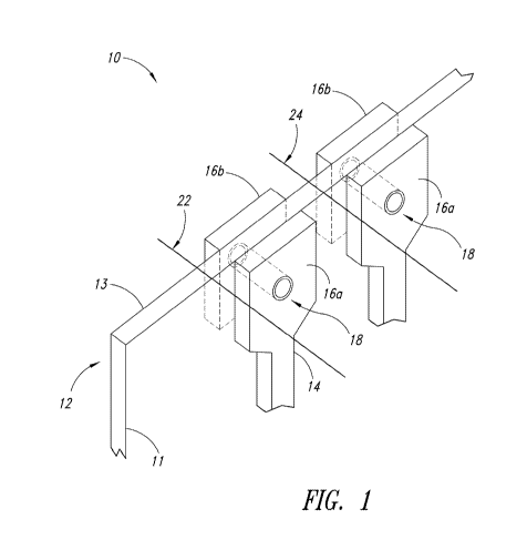
Figure 1 is a perspective view of at least one embodiment of a flex
circuit 10 for an acoustic stack in an ultrasound transducer. The flex circuit
10
includes an insulating layer 12, conductive traces 14, and conductive pads 16.
The insulating layer 12 is made of any suitable flexible insulating
material, such as polyimide. Conductive traces 14 are formed on a first
surface
11 (e.g., a front surface) of the insulating layer 12. The conductive traces
14
may be made of any conductive material and may be formed using any suitable
process, such as by deposition of the conductive material on the insulating
layer 12 using one or more masks or deposition patterns. In one or more
embodiments, the conductive traces 14 include copper.
Each of the conductive traces 14 formed on the first surface 11 of
the insulating layer 12 is coupled to a respective conductive pad 16a on the
first
surface 11. The conductive pads 16a may be formed in a same process, and
of a same material, as the conductive traces 14.
In the embodiment shown in Figure 1, each of the conductive
pads 16a on the first surface 11 of the insulating layer 12 is aligned with,
and
electrically coupled to, a respective conductive pad 16b that is formed on a
5
CA 03035915 2019-03-05
WO 2018/049222 PCT/US2017/050768
second surface 13 (e.g., a back surface) of the insulating layer 12. The
conductive pads 16a, 16b are electrically coupled to one another by a
conductive through-hole or via 18.
The via 18 is formed through the aligned, corresponding
conductive pads 16a on the first surface 11 and conductive pads 16b on the
second surface 13. A through-hole may be formed, for example, by drilling,
punching or the like through the aligned conductive pads 16a, 16b on the first
and second surfaces 11, 13 of the insulating layer 12, and the through-hole
may then be plated with a conductive material, such as copper. As such, the
vias 18 electrically couple respective conductive pads 16a, 16b through the
insulating layer 12. Accordingly, a signal provided through a trace 14 on the
first surface 11 of the insulating layer 12 is provided to a conductive pad
16a on
the first surface 11, as well as to a corresponding conductive pad 16b on the
second surface 13, through the via 18.
The flex circuit 10 thus provides redundant points of electrical
contact when attached to an acoustic stack. That is, the flex circuit 10 may
be
attached to the acoustic stack such that corresponding conductive pads 16a,
16b formed on each side of the insulating layer 12 are each in contact with a
respective transducer element in the acoustic stack. Additionally, since the
corresponding conductive pads 16a, 16b are electrically coupled to one another
by the conductive via 18, a signal provided through a trace 14 on the first
surface 11 of the insulating layer 12 will be transmitted to the respective
transducer element by the corresponding conductive pads on both surfaces 11,
13 of the insulating layer 12. Accordingly, transmission of a signal (e.g., a
driving signal) to a transducer element in an acoustic stack may be
facilitated
even in the event, for example, that one of the corresponding conductive pads
16a, 16b has a faulty connection with the transducer element or is in any way
deteriorated in its ability to carry an electrical signal.
The flex circuit 10 may be diced into individual conductive paths
using, for example, a dicing saw. The flex circuit 10 may be diced so that
each
of the conductive paths includes a respective conductive trace 14 and
6
CA 03035915 2019-03-05
WO 2018/049222
PCT/US2017/050768
corresponding conductive pads 16a, 16b formed on respective surfaces of the
insulating layer 12. The flex circuit 10 may be cut, for example, along dicing
lines 22, 24, as shown in Figure 1.
Figure 2 is a perspective view of a flex circuit 100 in accordance
with one or more alternative embodiments of the present disclosure. The flex
circuit 100 of Figure 2 is similar in structure and in function to the flex
circuit 10
of Figure 1, except for the differences that will be discussed below. The
features shared by the flex circuits 10 and 100 will not be described here
again
in the interest of brevity.
The main difference between the flex circuits 10 and 100 is that,
in the flex circuit 100 of Figure 2, conductive pads on the second surface 13
of
the insulating layer 12 are formed from a single conductive bus 116. The
conductive bus 116 may be formed, for example, of copper using a deposition
technique. Alternatively, the conductive bus 116 may be a prefabricated piece
of conductive material that is bonded to the second surface 13 of the
insulating
layer 12 using, for example, an adhesive. In one or more embodiments, the
conductive bus 116 has a height (h) of about 5 millimeters. The conductive bus
116 is formed on or bonded to an opposite surface of the insulating layer 12
(e.g., the second surface 13, as shown) as the conductive pads 16a. As in the
flex circuit 10 of Figure 1, conductive vias 18 are formed through the
conductive
pads 16a on the first surface 11 of the insulating layer 12, thereby
electrically
coupling the conductive pads 16a to corresponding regions of the conductive
bus 116 on the second surface 13 of the insulating layer 12.
The flex circuit 100 may then be diced into individual conductive
paths using a dicing saw and cutting, for example, along dicing lines 122,
124.
After dicing through the conductive bus 116 and the insulating layer 12, as
shown at dicing lines 122, 124, the flex circuit 100 includes individual
conductive paths made up of the traces 14 formed on the first surface 11 of
the
insulating layer, as well as conductive pads 16a on the first surface 11 and
corresponding conductive regions of the conductive bus 116 on the second
7
CA 03035915 2019-03-05
WO 2018/049222
PCT/US2017/050768
surface 13 (i.e., portions of the conductive bus 116 after dicing) that are
coupled to respective conductive pads 16a through the conductive vias 18.
FIG. 3A is a front view illustrating an ultrasound transducer
acoustic stack 200 including a flex circuit in accordance with one or more
embodiments of the present disclosure, and Figure 3B is a side view of the
acoustic stack 200 shown in Figure 3A.
The acoustic stack 200 includes a plurality of transducer elements
32, an acoustic matching layer 34, and a flex circuit 10. The flex circuit 10
is
attached to a lower surface of the transducer elements 32, and the acoustic
matching layer 34 is attached to an upper surface of the transducer elements
32.
The flex circuit 10, transducer elements 32, and acoustic
matching layer 34 may be attached to one another to form the acoustic stack
200 using an adhesive material, such as an epoxy. In one or more
embodiments, the transducer elements 32 are made of a piezoelectric material,
such as a piezoelectric ceramic material. The transducer elements 32 may
include electrodes (e.g., signal electrodes and/or ground electrodes) which
are
electrically coupled to the conductive pads 16a, 16b formed on the first and
second surfaces 11, 13, respectively, of the insulating layer 12.
Alternatively,
the transducer elements 32 may be electrically coupled to respective
conductive pads 16a, 16b by attaching the transducer elements 32 to the flex
circuit 10 with a conductive epoxy, solder, solder paste, or the like. The
flex
circuit 10 is attached to the transducer elements 32 in such a way that each
transducer element 32 is electrically coupled to two conductive pads 16a, 16b,
one on each surface 11, 13 of the insulating layer 12, thereby establishing
redundant points of contact for transmitting a signal from the associated
conductive trace 14 to the transducer element 32.
The acoustic block 200 shown in Figures 3A and 3B may be
formed by a variety of fabrication processes. In one embodiment, the
transducer elements 32 may be provided initially as a single block of
piezoelectric material. Similarly, the conductive pads 16a on the first
surface 11
8
CA 03035915 2019-03-05
WO 2018/049222 PCT/US2017/050768
of the insulating layer 12 and/or the conductive pads 16b on the second
surface
13 of the insulating layer 13 may initially be provided as a block of
conductive
material (e.g., the conductive bus 116 shown in Figure 2) electrically coupled
to
the respective traces 14 on the insulating layer 12.
Through-holes may be formed e.g., by drilling, punching or the
like, through the conductive bus 116 on the second surface 13 at locations
that
will be included in the conductive pads 16b, once formed. The through-holes
are formed to extend through the conductive bus 116, the insulating layer 12,
and the conductive pads 16a on the first surface 11 of the insulating layer
12.
The through-holes may then be plated or otherwise coated with a conductive
material, such as copper, to form the conductive vias 18 which electrically
couple the conductive pads 16a to associated regions of the conductive bus
116 that, after dicing, will become conductive pads 16b on the second surface
13 of the insulating layer 12.
The piezoelectric block may be attached to the flex circuit 10 such
that the conductive pads 16a on the first surface 11 and the conductive bus
116
on the second surface 13 are in contact with the piezoelectric block. The
piezoelectric block and the flex circuit 10 may then be diced into individual
transducer elements 32 and corresponding conductive pads 16a, 16b using a
dicing saw. As such, a plurality of individual transducer elements 32 may be
formed, with each transducer element 32 being electrically coupled to a pair
of
associated conductive pads 16a, 16b of the flex circuit 10. Each of the
conductive pads 16a is electrically coupled to a corresponding trace 14 formed
on the first surface 11 of the insulating layer 12, and each conductive pad
16a
is further coupled by a conductive via 18 to a respective conductive pad 16b
on
the second surface 13 of the insulating layer 12. Accordingly, a redundant
electrical connection is formed between the flex circuit 10 and the transducer
elements 32, as each trace 14 of the flex circuit 10 is coupled to a
conductive
pad 16a on the first surface 11 of the insulating layer 12, as well as to a
conductive pad 16b on the second surface 13 of the insulating layer 12.
9
CA 03035915 2019-03-05
WO 2018/049222
PCT/US2017/050768
After the piezoelectric block has been diced into individual
transducer elements 32, as described above, gaps formed between transducer
elements 32 and/or between adjacent conductive pads 16a, 16b of the flex
circuit 10 may be filled with an adhesive material, such as an epoxy filling
40.
The acoustic matching layer 34 may then be attached to an upper
surface of the transducer elements 32 and/or epoxy filling 40 using any
suitable
adhesive, such as an epoxy.
The conductive pads 16a on the first surface 11 of the insulating
layer 12 do not necessarily have the same dimensions as the corresponding
conductive pads 16b on the second surface 13 of the insulating layer 12. For
example, as shown in Figure 2, the conductive pads 16b may be formed by
dicing through the conductive bus 116, while the conductive pads 16a may be
already formed of suitable dimensions, along with the traces 14. In such a
case, the conductive pads 16b formed after dicing the flex circuit 10 may have
a
larger area dimension than the pre-formed conductive pads 16a.
In another embodiment, the transducer elements 32 may be
initially provided as a single block of piezoelectric material, while the flex
circuit
10 may have been previously cut into a plurality of traces 14 and associated
conductive pads 16a, 16b with conductive vias 18 formed through
corresponding conductive pads 16a, 16b. The pre-cut flex circuit 10 may be
attached to the piezoelectric block such that each associated pair of
conductive
pads 16a, 16b contacts the piezoelectric block at regions that will later be
cut
into individual transducer elements 32. The piezoelectric block is then diced
into individual transducer elements 32, for example, using a dicing saw.
In yet another embodiment, the acoustic stack 10 may be formed
from transducer elements 32 that have already been diced, and from the flex
circuit 10 that has also already been diced to form a plurality of traces 14
and
associated conductive pads 16a, 16b with conductive vias 18 formed through
corresponding conductive pads 16a, 16b. In such a case, the transducer
elements 32 may be directly attached or otherwise electrically coupled to
respective conductive pads 16a, 16b on the first and second surfaces 11, 13,
CA 03035915 2019-03-05
WO 2018/049222
PCT/US2017/050768
respectively, of the insulating layer 12. The epoxy filling 40 may be applied,
and the acoustic matching layer 34 may be attached to the transducer elements
32 as described herein.
The various features and elements of the embodiments described
above can be combined in additional ways to provide further embodiments.
These and other changes can be made to the embodiments in light of the
above-detailed description. In general, in the following claims, the terms
used
should not be construed to limit the claims to the specific embodiments
disclosed in the specification and the claims, but should be construed to
include
all possible embodiments along with the full scope of equivalents to which
such
claims are entitled. Accordingly, the claims are not limited by the
disclosure.
11