Sélection de la langue

Search

Sommaire du brevet 3039987 

Énoncé de désistement de responsabilité concernant l'information provenant de tiers

Une partie des informations de ce site Web a été fournie par des sources externes. Le gouvernement du Canada n'assume aucune responsabilité concernant la précision, l'actualité ou la fiabilité des informations fournies par les sources externes. Les utilisateurs qui désirent employer cette information devraient consulter directement la source des informations. Le contenu fourni par les sources externes n'est pas assujetti aux exigences sur les langues officielles, la protection des renseignements personnels et l'accessibilité.

Disponibilité de l'Abrégé et des Revendications

L'apparition de différences dans le texte et l'image des Revendications et de l'Abrégé dépend du moment auquel le document est publié. Les textes des Revendications et de l'Abrégé sont affichés :

  • lorsque la demande peut être examinée par le public;
  • lorsque le brevet est émis (délivrance).
(12) Demande de brevet: (11) CA 3039987
(54) Titre français: CIRCUIT DE COMMANDE DE DEMARRAGE ET DE VITESSE AUTOMATIQUE
(54) Titre anglais: AUTOMATIC START AND SPEED COMMAND CIRCUIT
Statut: Conforme
Données bibliographiques
(51) Classification internationale des brevets (CIB):
  • H02P 1/18 (2006.01)
  • H03K 17/687 (2006.01)
  • H03K 17/78 (2006.01)
(72) Inventeurs :
  • MASTROMATTEI, ANTHONY (Canada)
  • MASTROMATTEI, JORDAN LUIGI (Canada)
  • MASTROMATTEI, ROBERT ALDO (Canada)
(73) Titulaires :
  • MASTROMATTEI, ANTHONY (Canada)
  • MASTROMATTEI, JORDAN LUIGI (Canada)
  • MASTROMATTEI, ROBERT ALDO (Canada)
(71) Demandeurs :
  • MASTROMATTEI, ANTHONY (Canada)
  • MASTROMATTEI, JORDAN LUIGI (Canada)
  • MASTROMATTEI, ROBERT ALDO (Canada)
(74) Agent:
(74) Co-agent:
(45) Délivré:
(22) Date de dépôt: 2019-04-10
(41) Mise à la disponibilité du public: 2020-10-10
Licence disponible: S.O.
(25) Langue des documents déposés: Anglais

Traité de coopération en matière de brevets (PCT): Non

(30) Données de priorité de la demande: S.O.

Abrégés

Abrégé anglais


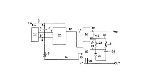
Automatic start and speed command circuit for supplying an analog start
acceleration and preset signal to an AC electric motor controlled by a
variable frequency motor and or brushed/brushless DC motor controller or
any electric motor speed control or drive which uses an analog speed
command signal input for supplying a variable analog speed command to
the controller for setting an operational motor speed. This includes
manually speed setting device such as potentiometer.
Automatic start and speed command circuit will provide a cycle start after
which will increase the command to said electric analog drive to accelerate
the motor for an allotted time to allow the controller and motor to
achieve the commanded speed at the motor, the speed command is
incrementally increased till maximum speed or set speed is
achieved.
A adjustable time base is included for each increase of command speed
to allow for tuning the start up performance of the motor. An isolated
power source is included which provides power to the circuit and is
isolated from the command signal on the drive or controller as not to
interfere with input command on the drive and/or controller.

Revendications

Note : Les revendications sont présentées dans la langue officielle dans laquelle elles ont été soumises.


CLAIMS

The embodiments of the invention in which an exclusive property or privilege
is
claimed are defined as follows:

1. In an automatic start and speed command apparatus for an electric
motor drive system;
(a ) An automatic start and speed command apparatus to provide automatic
start and speed command with a generated acceleration command reaching a
predetermined set point and after a predetermined time provide a second
command for the second set point whereas acting as a final speed for the
application based on the drive motor rating and the requirement of the
application.
(b) a drive means a electric motor control which maybe a brushed or brushless
DC motor, variable frequency drive, or a servo drive having an analog input
for
control.
(c) starting means to energize the motor by providing a start signal and a
speed
command in the case of brushless DC whereas the signal is provided by a
manually operated hall effect device or an adjustable resistor.
(d) a speed command signal means a signal to a drive which by its magnitude
relative to the input range of the drive will produce a speed in relation to
the
command.
(e) an electrical speed command control to energize the motor command signal
and having a predetermined speed and incremental steps during the
acceleration of the drive motor for achieving maximum or final set speed.
(f) means to run the speed command control only when the motor is stopped
and required to start.
(g) means to automatically provide a start command and incremental increase
in acceleration after the drive has been energized.
2. In the drive system of claim 1 wherein means to delay the running
speed of the drive is an electrical speed control after energizing of the
drive at
the beginning of each start cycle, switch means are actuated to energize the
electrical speed command control.
3. An automatic start and speed command apparatus of claim 1
comprising: Three Dual Solid State Relays comprises two independent, optically

coupled, bidirectional MOSFET switches for changing states of the signals as
described on Fig 3 and a 555 timer to provide a preset time delay for two of
said switches and connected to a node comprising of resistive capacitive
series


network and a node of series connected resistive element and capacitive
element to provide automatic generation of a start and acceleration command
signal connected to an adjustable 555 timer to provide timing for the
initiation
of the run speed for the drive and motor connected to the circuit and in
operative association with an electric motor controller with an analog input
with a reference for accepting speed commands relative to the drives internal
reference voltage.
4. The automatic start and speed command apparatus of claim 2 where
the external start connected to the input of the first dual solid state relay
comprises two independent, optically coupled, bidirectional MOSFET switches
with the first contact having a normally closed contact and electrically
connected to a node consisting of a capacitor and is coupled to both the
trigger
and threshold inputs of said 555 timer and the second normally closed contact
electrically connected to the node and the said discharge connection varying
the voltage at the node in synchronism with a change in the logic state output

signals of said 555 timer.
5. The automatic start and speed command apparatus of claim 2
wherein the first of two Dual Solid State Relays comprises two independent,
optically coupled, bidirectional MOSFET switches for initiating an automatic
generation of a ramping command signal connected to an adjustable resistive
capacitive network to provide said optically coupled, bidirectional MOSFET
switch, contact closure allowing signal to start and accelerate and a 555
timer
to provide timing for the initiation of a second set point setting for the run

speed and adjustable resistive element and at the same node the final output
command to the drive. The command follows the charging curve of the
capacitor till it reaches the maximum value which is the first speed command
for the first setting.
6. The automatic start and speed command apparatus of claim 2
wherein the second of two Dual Solid State Relays (SSR) comprises two
independent, optically coupled, bidirectional MOSFET switches for switching to

the second set point by energizing the input from the output command signal
connected to the 555 timer circuit with a set preselected value for generating
a
specified time delay to energize the inputs of both of the Dual Solid State
Relay
comprising of two independent, optically coupled, bidirectional MOSFET switch
and the second Dual Solid State Relay comprising of two independent, optically


coupled, bidirectional MOSFET switch; and second set point is provided when
the optically isolated relay of the first bidirectional MOSFET switch is
energized
and the contacts open on the first bidirectional MOSFET switch, and the
normally open contacts close according to the configuration of said relay; and

when the normally open contact closes a second voltages at the node which is
electrically connected to the resistor and Zener diode and further wherein the

resistor and the Zener diode coupled between the speed command output to
the speed input of the drive.

Description

Note : Les descriptions sont présentées dans la langue officielle dans laquelle elles ont été soumises.


1
AUTOMATIC START AND SPEED COMMAND CIRCUIT
BACKGROUND
This invention relates to a start and speed command circuit and, more
particularly to a speed command control that provides a continuous
increase in acceleration to a set point for starting and further set point
speed command to a final set point speed after the starting of an electrical
motor drive control.
DESCRIPTION OF PRIOR ART
Start and speed command developments are required in many applications
to determine start and speed command levels to insure proper operation
of equipment. Traditionally, speed command has been accomplished by
hall affect and manual settings that rely upon manual input changes of the
device in response to start and speed command changes of the electrical
motor drive. These electrical motor controlling devices require manual
operation and vary from their designed commanded operational
characteristics. One object of the present invention is to provide an
automatic reliable electrical motor drive automatic start and speed
command signal for starting and running speed.
SUMMARY OF THE INVENTION
This invention includes a start and speed command circuit that provides a
start control system and speed stepped approach to starting and speed
setting for the drive. These controls are utilized by devices to increase the
efficiency of the motors and hence the systems and devices that use them.
Both DC and AC drive systems are used to provide efficient and proper
operation during normal conditions, and maintain proper and safe use. The
frequency of or, expressed alternatively, the interval between successive
increase speed commands is selected to prevent stalling and excessive
current draw under heavy usage conditions. For example, Variable
Frequency Drives permit the user to optimize the control speeds based on
a particular AC motor characteristic and usage conditions.
CA 3039987 2019-04-10

BRIEF DESCRIPTION OF THE DRAWINGS
The features and advantages of this invention mentioned above will
become more apparent as the invention becomes better understood by
the detailed that follows, when considered in connection with the
submitted drawings.
FIGURE 1 is a schematic diagram of the auto start and speed
command circuit.
FIGURE 2 is an overview of the auto start and speed command
circuit output to the electric motor drive.
FIGURE 3 is a timing chart of the output signals produced by the
auto start and speed command circuit.
DESCRIPTION OF THE PREFERRED EMBODIMENT
This invention includes a start and speed command circuit with two speed
transition points one transition point provides an start to a preset speed
set point transition command and the second set point is the transition to
maximum preset speed. Externally started speed command. Fig 3 is the
schematic diagram of the embodiment of this invention. Connected to two
Dual Solid State Relay (SSR) comprises two independent, optically coupled,
bidirectional MOSFET switches. The first having a normally closed switch
and coupled to it a node consisting of a capacitor and resistive element and
at the same node the final output command to the drive. The command
follows the charging curve of the capacitor till it reaches the maximum
value which is the first speed command for the first setting. During which
Fig 1 (10) a 555 timer having it's trigger inputs coupled to the node of the
voltage divider resistive and capacitance timing sensing node of the said
555 timer outputting the time base of switching the command relays relay
logic state when energized opens the first bidirectional MOSFET switch and
closes the switch of the second bidirectional MOSFET switch and having a
resister element electrically connected to the Zener diode which is
electrically connected to the node of the final output and providing a
CA 3039987 2019-04-10

command voltage on the said node in accordance to the voltage of the
Zener reversed bias voltage.
2. The circuit starts when the input is applied to Fig. 1 (1) as a start
signal with a switch closure closes the switch of the first bidirectional
MOSFET switch Fig. 1 (10) and power is provided to Fig 1 (7) of the Fig 1
(20) 555 timer and at this time the capacitor is discharged therefore there
is 0 volts at the Fig 1 (8) Threshold which is the positive input to the
second
internal comparator in the 555 timer semiconductor Fig 1 (10) and since
the V+ input is lower than the negative side of the internal comparator
input the output stays low and does not trigger the input of the internal flip
flop.
3. When we switch the Trigger input Fig 1 (7) of the 555 timer and
the input is pulled low this will provide V- 0 volts to the negative input of
the Fig 1 (10) 555 timer's said first comparator and the V+ is higher than
the negative input on the comparator which turns the output high which is
tied to the internal flip flop set input and the flip flop is triggered and
the
output of Fig 1 555 timer (10) 12 output is driven high by the flip flop and
said output provides a positive input to both and Fig 1 (30) and Fig 1 (40)
Dual Solid State Relays, optically coupled, bidirectional MOSFET switch the
first and second opto-isolated relays.
4. The Dual Solid State Relay, optically coupled, bidirectional MOSFET
switches. This normally open switch, from the Fig 1 (30) dual OptoMOS
Relay provides both switches the first is normally open and the second is
normally closed and configured as a single pole double throw
configuration. When the Fig 1 (30) and Fig 1 (40) inputs are in the off
condition the first optically coupled, bidirectional MOSFET switch is
normally closed and the external command reference is connected to the
switch which feeds the resistive capacitor elements and causes the
CA 3039987 2019-04-10

capacitor Fig 1 (25) to charge while the output voltage increases which
causes a ramping effect in respect to the charging curve of said capacitor
Fig 1 (25) and the signal increases during the timing of the input to the 555
timer Fig 1 (20) and when the output from the timer is turned on the
optically coupled, bidirectional MOSFET switch Fig 1 (30) and Fig 1 (40)
which are coupled on the node receives a positive input and the output of
the first bidirectional MOSFET switch opens and the output of switch one is
off and the second bidirectional MOSFET switch closes and the output of
the second bidirectional MOSFET switch provides a voltage to the output
coupled to node at Fig 1 (23)resistive element and Fig 1 (26) Zener diode.
5. The Fig 1 (26) Zener diode is driven in reverse bias till the reverse
output of the diode is reached and provides the maximum output value for
the circuit.
6. The fifth bidirectional MOSFET relay signal Fig 1 (30) and sixth Fig 1
(40) bidirectional MOSFET relay signal is turned off by the external process;
the internal switches open on the first relay which removes the start signal
from the Fig 1 (20) 555 timer trigger Fig 1 (20) 7 and the sixth bidirectional

MOSFET relay closes when de-energized and makes the connection
between on the node Fig 1 (20) 7 which has a value of 0 volts as the
internal discharge transistor of is on Fig 1 (20) and the transistor output is

at 0 volts the Discharge signal on the Fig
1 (20) 555 timer and Fig 1 (20) 8 the threshold pin which is tied to the
second comparator V+ Fig 1 (20) 555 timer now is low which is lower than
the V- input of the second comparator Fig 1 (20) 555 timer and the output
is turned off to the Fig 1 (20) 555 timer flip flop and the circuit resets.
CA 3039987 2019-04-10

Dessin représentatif
Une figure unique qui représente un dessin illustrant l'invention.
États administratifs

Pour une meilleure compréhension de l'état de la demande ou brevet qui figure sur cette page, la rubrique Mise en garde , et les descriptions de Brevet , États administratifs , Taxes périodiques et Historique des paiements devraient être consultées.

États administratifs

Titre Date
Date de délivrance prévu Non disponible
(22) Dépôt 2019-04-10
(41) Mise à la disponibilité du public 2020-10-10

Historique d'abandonnement

Il n'y a pas d'historique d'abandonnement

Taxes périodiques

Dernier paiement au montant de 50,00 $ a été reçu le 2020-04-27


 Montants des taxes pour le maintien en état à venir

Description Date Montant
Prochain paiement si taxe applicable aux petites entités 2024-04-10 100,00 $
Prochain paiement si taxe générale 2024-04-10 277,00 $

Avis : Si le paiement en totalité n'a pas été reçu au plus tard à la date indiquée, une taxe supplémentaire peut être imposée, soit une des taxes suivantes :

  • taxe de rétablissement ;
  • taxe pour paiement en souffrance ; ou
  • taxe additionnelle pour le renversement d'une péremption réputée.

Les taxes sur les brevets sont ajustées au 1er janvier de chaque année. Les montants ci-dessus sont les montants actuels s'ils sont reçus au plus tard le 31 décembre de l'année en cours.
Veuillez vous référer à la page web des taxes sur les brevets de l'OPIC pour voir tous les montants actuels des taxes.

Historique des paiements

Type de taxes Anniversaire Échéance Montant payé Date payée
Le dépôt d'une demande de brevet 200,00 $ 2019-04-10
Taxe de maintien en état - Demande - nouvelle loi 2 2021-04-12 50,00 $ 2020-04-27
Taxe de maintien en état - Demande - nouvelle loi 3 2022-04-11 50,00 $ 2020-04-27
Taxe de maintien en état - Demande - nouvelle loi 4 2023-04-11 50,00 $ 2020-04-27
Titulaires au dossier

Les titulaires actuels et antérieures au dossier sont affichés en ordre alphabétique.

Titulaires actuels au dossier
MASTROMATTEI, ANTHONY
MASTROMATTEI, JORDAN LUIGI
MASTROMATTEI, ROBERT ALDO
Titulaires antérieures au dossier
S.O.
Les propriétaires antérieurs qui ne figurent pas dans la liste des « Propriétaires au dossier » apparaîtront dans d'autres documents au dossier.
Documents

Pour visionner les fichiers sélectionnés, entrer le code reCAPTCHA :


Pour visualiser une image, cliquer sur un lien dans la colonne description du document. Pour télécharger l'image (les images), cliquer l'une ou plusieurs cases à cocher dans la première colonne et ensuite cliquer sur le bouton "Télécharger sélection en format PDF (archive Zip)" ou le bouton "Télécharger sélection (en un fichier PDF fusionné)".

Liste des documents de brevet publiés et non publiés sur la BDBC .

Si vous avez des difficultés à accéder au contenu, veuillez communiquer avec le Centre de services à la clientèle au 1-866-997-1936, ou envoyer un courriel au Centre de service à la clientèle de l'OPIC.


Description du
Document 
Date
(yyyy-mm-dd) 
Nombre de pages   Taille de l'image (Ko) 
Paiement de taxe périodique 2020-04-27 3 65
Changement à la méthode de correspondance 2020-04-27 3 65
Dessins représentatifs 2020-08-31 1 6
Page couverture 2020-08-31 2 46
Modification au demandeur/inventeur 2020-11-09 1 28
Changement/correction de nom refusée 2021-01-07 2 182
Lettre du bureau 2021-03-03 2 210
Abrégé 2019-04-10 1 27
Description 2019-04-10 4 162
Revendications 2019-04-10 3 105
Dessins 2019-04-10 2 21
Lettre de courtoisie 2019-04-26 2 73