Note : Les descriptions sont présentées dans la langue officielle dans laquelle elles ont été soumises.
CA 03096679 2020-10-08
WO 2019/209604 PCT/US2019/028000
TRANSMIT AND RECEIVE SWITCH AND BROADBAND POWER AMPLIFIER
MATCHING NETWORK FOR MULTI-BAND MILLIMETER-WAVE SG
COMMUNICATION
CROSS REFERENCE
[0001] This application claims benefit of the U.S. Non-Provisional
Application No.
15/965,694 filed on April 27, 2018.
FIELD OF THE INVENTION
[0002] Embodiments of the present invention relate generally to wireless
communication
devices. More particularly, embodiments of the invention relate to a
transmit/receive switch
and a broadband power amplifier matching network of a communication device.
BACKGROUND
100031 The 5G communication requires wide-band operation at the frequency
range from
24GHz to 43GHz, necessitating a wide-band and efficient wireless transmitter.
Conventionally, power amplifier (PA) and transmit/receive (T/R) switch are
designed
separately with a single standard 500 interface. The separation of these
circuits can result in
sacrificed transmitter bandwidth, output power, and efficiency.
[0004] Major transmitter specifications (for example, bandwidth, output
power, and
efficiency) are substantially governed or dominated by components located past
the PA active
transistors, for example, the PA output matching network and the T/R switch.
Therefore, co-
design of the PA output matching networks and T/R switch can provide a unique
advantage
and benefit to improve transmitter performance.
CA 03096679 2020-10-08
WO 2019/209604 PCT/US2019/028000
[0005] Furthermore, a T/R switch can beneficially have a greater degree of
design
freedom and improved impedance matching if the transmit and receive branches
have
separate matching inductors.
BRIEF DESCRIPTION OF THE DRAWINGS
[0006] Embodiments of the invention are illustrated by way of example and
not limitation
in the figures of the accompanying drawings in which like references indicate
similar
elements
[0007] Figure I is a block diagram illustrating an example of a wireless
communication
device according one embodiment.
[0008] Figure 2 is a block diagram illustrating an example of an RF
frontend integrated
circuit according to one embodiment.
[0009] Figure 3 is a block diagram illustrating an RF frontend integrated
circuit according
to one embodiment.
[0010] Figure 4 is a block diagram illustrating an example of a power
amplifier integrated
circuit according to one embodiment
100111 Figure 5 shows a PA output matching network and a T/R switch
according to one
embodiment.
[0012] Figure 6 shows a PA output matching network and a T/R switch
according to one
embodiment.
[0013] Figure 7, graphs a-c show a comparison between an output matching
circuit by
itself and an output matching circuit connected to a T/R switch.
100141 Figure 8, graphs a-c show real impedance, imaginary impedance, and
passive loss
of a co-designed output matching circuit and T/R switch.
[0015] Figure 9 shows an embodiment of the T/R switch
2
CA 03096679 2020-10-08
WO 2019/209604 PCT/US2019/028000
BRIEF DESCRIPTION OF THE DRAWINGS
[0016] Embodiments of the invention are illustrated by way of example and
not limitation
in the figures of the accompanying drawings in which like references indicate
similar
elements
[0017] Figure 1 is a block diagram illustrating an example of a wireless
communication
device according one embodiment.
[0018] Figure 2 is a block diagram illustrating an example of an RE
frontend integrated
circuit according to one embodiment.
[0019] Figure 3 is a block diagram illustrating an RF frontend integrated
circuit according
to one embodiment.
[0020] Figure 4 is a block diagram illustrating an example of a power
amplifier integrated
circuit according to one embodiment.
[0021] Figure 5 shows a PA output matching network and a T/R switch
according to one
embodiment.
[0022] Figure 6 shows a PA output matching network and a T/R switch
according to one
embodiment.
[0023] Figure 7, graphs a-c show a comparison between an output matching
circuit by
itself and an output matching circuit connected to a T/R switch.
[0024] Figure 8, graphs a-c show real impedance, imaginary impedance, and
passive loss
of a co-designed output matching circuit and T/R switch.
[0025] Figure 9 shows an embodiment of the T/R switch.
3
DETAILED DESCRIPTION
[0026] Various embodiments and aspects of the inventions will be described
with
reference to details discussed below, and the accompanying drawings will
illustrate
the various embodiments. The following description and drawings are
illustrative of
the invention and are not to be construed as limiting the invention. Numerous
specific
details are described to provide a thorough understanding of various
embodiments of
the present invention. However, in certain instances, well-known or
conventional
details are not described in order to provide a concise discussion of
embodiments of
the present inventions.
[0027] Reference in the specification to "one embodiment" or "an
embodiment"
means that a particular feature, structure, or characteristic described in
conjunction
with the embodiment can be included in at least one embodiment of the
invention.
The appearances of the phrase "in one embodiment" in various places in the
specification do not necessarily all refer to the same embodiment.
[0028] According to some embodiments, an electronic circuit for wireless
communication includes a transmit/receive (T/R) switch. The T/R switch can
include
a transmit switch, between a transmit port and an antenna port; a receive
switch,
between a receive port and the antenna port; a transmit inductor, coupled in
parallel
between the transmit switch the transmit port; and a receive inductor, coupled
in
parallel between the transmit switch the transmit port.
[0028a] According to some embodiments, a radio frequency (RF) front end
circuit for
wireless communication, can include: a transmit/receive (T/R) switch, the T/R
switch
including: a transmit switch, between a transmit port and an antenna port; a
receive
switch, between a receive port and the antenna port; a transmit inductor,
coupled in
parallel between the transmit switch the transmit port; and a receive
inductor, coupled
in parallel between the transmit switch the transmit port.
4
CA 3096679 2020-11-06
-
[0029] According to some embodiments, an electronic circuit for wireless
communication can be a co-designed circuit with a T/R switch and a power
amplifier
matching network. The matching network can include a first capacitor coupled,
in
parallel, to an input port of the matching network circuit; a broadband on-
chip
transformer coupled, in parallel, to the first capacitor; and a second
capacitor coupled,
in series, in between the broadband on-chip transformer and an output port of
the
matching network circuit, wherein the output port of the matching network
circuit is
coupled to the transmit port of the T/R switch.
4a
CA 3096679 2020-11-06
CA 03096679 2020-10-08
WO 2019/209604 PCT/US2019/028000
100301 According to some embodiments, a matching network circuit includes a
first
capacitor coupled, in parallel, to an input port of the matching network
circuit; a broadband
on-chip transformer coupled, in parallel, to the first capacitor, where the
broadband on-chip
transformer includes a primary winding and a secondary winding, where the
secondary
winding is a partial winding. The matching network circuit includes a second
capacitor
coupled, in series, in between the broadband on-chip transformer and an output
port of the
matching network circuit
[0031] In one aspect, the primary and the secondary windings of the
broadband on-chip
transformer include planar octagonal windings. In another embodiment, the
planar octagonal
winding of the primary winding are electromagnetically coupled to the planar
octagonal
winding of the secondary windings along a planar axis. In another embodiment,
the primary
and the secondary windings are separated by a layer of dielectric. The primary
and secondary
windings may be disposed on different substrate layers as a part of an
integrated circuit (IC).
[0032] In one embodiment, the partial winding of the secondary winding
includes
approximately 1.5 turns winding. In one embodiment, the primary winding is
coupled to a
power supply source to supply a bias voltage to a circuit of the input port.
In one embodiment,
the secondary winding includes at least two conductive layers.
[0033] According to another aspect, a two-stage power amplifier (PA)
includes a first
amplifier stage, a second amplifier stage, a first matching network circuit
coupled in between
the first amplifier stage and the second amplifier stage, and a second
matching network circuit
coupled to an output port of the second amplifier stage. The second matching
network
includes a first capacitor coupled, in parallel, to an input port of the
second matching network
circuit; a broadband on-chip transformer coupled, in parallel, to the first
capacitor, where the
broadband on-chip transformer includes a primary winding and a secondary
winding, where
the secondary winding is a partial winding. The primary and secondary windings
may be
disposed on different substrate layers as a part of an integrated circuit. The
second matching
CA 03096679 2020-10-08
WO 2019/209604 PCT/US2019/028000
network includes a second capacitor coupled, in series, in between the
broadband on-chip
transformer and an output port of the second matching network circuit.
[0034] According to another aspect, an RF frontend integrated circuit (IC)
device includes
a two-stage power amplifier (PA) to amplify a transmitted signal. The PA
includes a first
amplifier stage, a second amplifier stage, a first matching network circuit
coupled in between
the first amplifier stage and the second amplifier stage, and a second
matching network circuit
coupled to an output port of the second amplifier stage. The second matching
network
includes a first capacitor coupled, in parallel, to an input port of the
second matching network
circuit; a broadband on-chip transformer coupled, in parallel, to the first
capacitor, where the
broadband on-chip transformer includes a primary winding and a secondary
winding, where
the secondary winding is a partial winding. The primary and secondary windings
may be
disposed on different substrate layers as a part of an integrated circuit. The
second matching
network includes a second capacitor coupled, in series, in between the
broadband on-chip
transformer and an output port of the second matching network circuit.
[0035] Figure 1 is a block diagram illustrating an example of a wireless
communication
device according one embodiment of the invention. Referring to Figure 1,
wireless
communication device 100, also simply referred to as a wireless device,
includes, amongst
others, an RF frontend module 101 and a baseband processor 102. Wireless
device 100 can be
any kind of wireless communication devices such as, for example, mobile
phones, laptops,
tablets, network appliance devices (e.g., Internet of thing or JOT appliance
devices), etc.
[0036] In a radio receiver circuit, the RF frontend is a generic term for
all the circuitry
between the antenna up to and including the mixer stage. It consists of all
the components in
the receiver that process the signal at the original incoming radio frequency,
before it is
converted to a lower intermediate frequency (IF). In microwave and satellite
receivers it is
often called the low-noise block (LNB) or low-noise downconverter (LND) and is
often
located at the antenna, so that the signal from the antenna can be transferred
to the rest of the
6
CA 03096679 2020-10-08
WO 2019/209604 PCT/US2019/028000
receiver at the more easily handled intermediate frequency. A baseband
processor is a device
(a chip or part of a chip) in a network interface that manages all the radio
functions (all
functions that require an antenna).
100371 In one embodiment, RF frontend module 101 includes one or more RF
transceivers, where each of the RF transceivers transmits and receives RF
signals within a
particular frequency band (e.g., a particular range of frequencies such as non-
overlapped
frequency ranges) via one of a number of RF antennas. The RF frontend IC chip
further
includes a frequency synthesizer coupled to the RF transceivers. The frequency
synthesizer
generates and provides a local oscillator (LO) signal to each of the RF
transceivers to enable
the RF transceiver to mix, modulate, and/or demodulate RF signals within a
corresponding
frequency band. The RF transceivers and the frequency synthesizer may be
integrated within
a single IC chip as a single RF frontend IC chip or package.
100381 Figure 2 is a block diagram illustrating an example of an RF
frontend integrated
circuit according to one embodiment of the invention. Referring to Figure 2,
RF frontend 101
includes, amongst others, a frequency synthesizer 200 coupled to a multi-band
RF transceiver
211. Transceiver 211 is configured to transmit and receive RF signals within
one or more
frequency bands or a broad range of RF frequencies via RF antenna 221. In one
embodiment,
transceiver 211 is configured to receive one or more LO signals from frequency
synthesizer
200. The LO signals are generated for the one or more corresponding frequency
bands. The
LO signals are utilized to mix, modulate, demodulated by the transceiver for
the purpose of
transmitting and receiving RF signals within corresponding frequency bands.
Although there
is only one transceiver and antenna shown, multiple pairs of transceivers and
antennas can be
implemented, one for each frequency bands.
[0039] Figure 3 is a block diagram illustrating an RF frontend integrated
circuit according
to one embodiment. Referring to Figure 3, frequency synthesizer 300 may
represent
frequency synthesizer 200 as described above. In one embodiment, frequency
synthesizer 300
CA 03096679 2020-10-08
WO 2019/209604 PCT/US2019/028000
is communicatively coupled to a broadband transmitter 301 and a broadband
receiver 302,
which may be a part of a transceiver such as transceiver 211. The broadband
transmitter 301
transmits RF for a number of frequency bands.
[0040] In one embodiment, transmitter 301 includes filters 303, mixers 304,
and a power
amplifier 305. Filters 303 may be one or more low-pass (LP) filters that
receives transmitting
(TX) signals to be transmitted to a destination, where the TX signals may be
provided from a
baseband processor such as baseband processor 102. Mixers 301 (also referred
to as up-
convert mixers) are configured to mix and modulate the TX signals onto one or
more carrier
frequency signal based on local oscillator (LO) signals provided by frequency
synthesizer
300. The modulated signals are then amplified by power amplifier 305 and the
amplified
signals are then transmitted to a remote receiver via antenna 310.
[0041] The RF frontend integrated circuit can include a receiver 302.
Receiver 302
includes a low noise amplifier (LNA) 306, mixer(s) 307, and filter(s) 308. LNA
306 is to
receive RF signals from a remote transmitter via antenna 310 and to amplify
the received RF
signals. The amplified RF signals are then demodulated by mixer(s) 307 (also
referred to as a
down-convert mixer) based on a LO signal provided by frequency synthesizer
300. The
demodulated signals are then processed by filter(s) 308, which may be a low-
pass filter. In
one embodiment, transmitter 301 and receiver 302 share antenna 310 via a
transmitting and
receiving (T/R) switch 309. T/R switch 309 is configured to switch between
transmitter 301
and receiver 302 to couple antenna 310 to either transmitter 301 or receiver
302 at a particular
point in time. Although there is only one pair of transmitter and receiver
shown, multiple pairs
of transmitters and receivers may be coupled to frequency synthesizer 300, one
for each of the
multiple frequency bands.
[0042] Figure 4 is a block diagram illustrating an example of a power
amplifier (PA)
integrated circuit according to one embodiment. Referring to Figure 4, PA 400
can be PA 305
of Figure 3. PA 400 can include driver stage 401, inter-stage matching network
402, output
8
CA 03096679 2020-10-08
WO 2019/209604 PCT/US2019/028000
stage 403, and output matching network 404. Inter-stage matching network 402
and output
matching network 404 can match impedances seen by driver stage 401 and output
stage 403
to maximize a power transfer for PA 400. For example, inter-stage matching
network 402 can
match an input impedance and an output impedance to an impedance seen at the
output port
of driver stage 401 and an impedance seen at the input port of output stage
403, respectively,
to maximize a power transfer from an input port of PA 400 to the output stage
403. Output
matching network 404 can match the impedance seen from an output port of
output stage 403
to maximize a power transfer from the output stage 403 to the output port of
PA 400. Lastly,
output matching network 404 can provide differential to single-ended
conversion for a single-
ended output port of PA 400.
100431 Referring to Figure 4, driver stage 401 and output stage 403 are
amplifier stages of
PA 400. In one embodiment, driver stage 401 and output stage 403 are
differential cascode
amplifier stages. A differential amplifier is an amplifier that amplifies a
difference between
two input voltages but suppresses any voltage common to the two inputs.
Differential
amplifiers offer common-mode noise rejection such as noise from nearby
components and
power supplies. A cascode amplifier is a two-stage amplifier (e.g., FETs or
BJTs) that
includes of a common-source (or a common-emitter for BJTs) stage feeding into
a common-
gate (or a common-base for BJTs) stage. Compared with single-stage amplifiers,
cascode
amplifiers have a higher input output isolation (i.e., reduces a leakage in
reverse transmission
from the output to the input ports as there is no direct coupling between the
input and output
ports), a higher input impedance, a higher output impedance, a higher gain,
and a
higher bandwidth. Here, driver stage 401 and output stage 403 include
amplifiers that
combine a differential topology and a cascode topology to achieve a large
output swing, a
wide bandwidth, with a high output power.
Transmit/Receive Switch
9
CA 03096679 2020-10-08
WO 2019/209604 PCT/US2019/028000
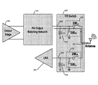
[0044] Referring now to FIG. 5, a transmit inductor I-Tx 903 can be coupled
in parallel
between the transmit switch 901 and the transmit port 905. Similarly, a
receive inductor 1_,Rx
904 can be coupled in parallel between the receive switch 902 and the receive
port 906.
[0045] The transmit switch 901 and the receive switch 902 can each have two
poles,
operating in sync, such that when a first pole of the transmit switch is
on/closed, thereby
connecting the output stage to the antenna, a first pole of the receive switch
is off/open,
thereby disconnecting the LNA from the antenna. Simultaneously, a second pole
of the
transmit switch is off/open, and a second pole of the receive switch is
on/closed, thereby
grounding the input to the LNA.
[0046] In one embodiment, as shown in FIG. 9, the poles of the transmit and
receive
switches 901 and 902 each comprise one or more mosfets, having control inputs
that are
alternatingly synced by Vail 1301 and inverse Vein 1302 to control the poles
as described
above.
[0047] Beneficially, 1_,Tx and 1_,Rx can be sized to optimize the impedance
matching in the
TX and RX paths. Separate inductors 1_,Tx and I.Rx, rather than a single
inductor at the antenna
907, provide an additional design freedom to optimize the bandwidth and
insertion loss in the
TX and RX paths Therefore, it is noted that, in one embodiment, there is no
inductor at the
antenna 907.
Co-Designed T/R Switch and PA output matching stage
[0048] Beneficially, because the inductors are separate, they can be co-
designed
separately with the transmit and receive circuit. For example, the transmit
inductor l_frx can be
co-designed with the PA output matching network 404, while the LRx can be co-
designed
with the LNA 306.
[0049] Furthermore, the PA output matching network can be implemented using
LC
lumped elements, transformers, or transmission-line-based distributed
components. To reduce
CA 03096679 2020-10-08
WO 2019/209604 PCT/US2019/028000
chip area, the PA output matching network 404 uses a transformer-based
matching network
with two tuning capacitors, which only occupies a single inductor footprint.
[0050] The lumped model equivalent circuit of the broadband output matching
network is
shown in Fig. 6. The PA output matching network 404 consists of an on-chip
transformer 501,
device parasitic capacitor Cd,, and two extra MOM capacitors Cp and C,. The
physical
transformer is modeled by an ideal transformer with its magnetizing inductor
and leakage
inductor, and its parasitic capacitors shunt to ground (Cparl and Cpar2). 1
Here, k is the magnetic
coupling coefficient, n is the turn radio, Lp is primary self-inductance. Rp
and R, models the
loss of the transformer.
[0051] For the T/R switch, Ron 911, 914 models the on-resistance of the
switch transistor
and Coif 913, 913 models the off-capacitance of the switch transistor.
[0052] A high-order passive network is formed to enable an instantaneously
broad
bandwidth. Thus, in a co-designed circuit, the value of each circuit element
is chosen to
achieve optimum load impedance seen by the PA output stage (Ropt) over the
operation
bandwidth while maintaining low insertion loss.
[0053] The gain of the PA output stage is defined as gm=IZI=Loss, where gm
is the
transconductance of the transistor, Z is the load impedance presented to the
PA output stage,
and Loss is the passive loss of the output matching network. The goal of the
broadband
matching is to achieve relatively constant power gain across the operation
frequency. Since
gm is frequency independent, this transforms the design goal to achieve
relatively constant Z1
and Loss over a broad bandwidth. In addition, PA transistors require real-
value Z to achieve
maximum output power and efficiency (load-pull condition), meaning that the
real part of Z
should be close to Ropt 1010 with imaginary part close to 0 across the
operation frequency.
[0054] If the PA output matching is designed for 500 antenna impedance
without
considering the effect from the T/R SW at the beginning, its in-band Z
variation and Loss
variation become larger after putting together with T/R SW in the systems
integration. For
11
CA 03096679 2020-10-08
WO 2019/209604 PCT/US2019/028000
example, the loss variation of the PA output matching network itself is 0.4dB
without adding
the T/R SW and increases to 1.8dB after integration with the T/R SW, as shown
in FIG. 7,
graph c.
[0055] Indeed, FIG. 7, graphs a-c show simulated load impedance seen by the
differential
output stage and simulated passive loss. In this simulation, the PA output
matching network is
originally designed for 500 antenna impedance without considering the T/R SW.
After
adding the T/R SW, the in-band impedance variation and loss variation becomes
larger.
[0056] Therefore, it is important to consider the parasitic capacitor
(Coff) of the T/R
Switch from the beginning and absorb it into the passive network synthesis by
building a co-
designed circuit, for example, by building a co-designed T/R switch and output
matching
circuit. The transformer parameters (k, n, and Lp), two tuning capacitors (Cp
and Cs), and
T/R SW TX-path inductor LTX are co-designed to achieve broadband matching.
[0057] Referring now to Fig. 8, a simulated load impedance seen by the
differential output
stage and simulated passive loss by co-designing the PA output matching
network with T/R
SW is shown in graphs a-c. The co-designed output matching circuit and T/R
switch has a real
part of the load impedance close to 500, and an imaginary part of the load
impedance close to
0. The in-band passive loss variation is 0.8dB.
100581 In the foregoing specification, embodiments of the invention have
been described
with reference to specific exemplary embodiments thereof. It will be evident
that various
modifications may be made thereto without departing from the broader spirit
and scope of the
invention as set forth in the following claims. The specification and drawings
are,
accordingly, to be regarded in an illustrative sense rather than a restrictive
sense.
12