Note : Les descriptions sont présentées dans la langue officielle dans laquelle elles ont été soumises.
CA 031.10470 2021-02-23
DESCRIPTION
CONTROL DEVICE, CONTROL DEVICE SYSTEM, RUNWAY FLASH LIGHTING
DEVICE CONTROL SYSTEM, PROGRAM, AND RECORDING MEDIUM
TECHNICAL FIELD
[0001] The present invention relates to a control device, a control device
system, a runway
flash lighting device control system, a program, and a recording medium.
BACKGROUND ART
[0002] Conventionally, flash lighting devices have been used to guide an
aircraft approaching a
runway when touching down at an airport. The control of the flash lighting
device is performed
by a system in which a control master station and a control slave station
transmit and receive
control signals to and from each other by wired signals (Patent Literature 1).
Citation List
Patent Literature
[0003] Patent Literature 1:JP 2002-362498 A
SUMMARY OF INVENTION
Technical Problem
[0004] However, signal processing without being affected by the noise is
required for
controlling the flash lighting device. This problem is not limited to the
control of the flash
lighting device, and the same problem also arises in traffic signals, train
signals, and the like in
which signal processing without being affected by the noise is required, for
example.
[0005] With the foregoing in mind, it is an object of the present invention to
provide a control
device that can perform signal processing without being affected by the noise
and a control
device system using the same.
Solution to Problem
[0006] In order to achieve the above object, the present invention provides a
first control device
including: a control signal transmitter; a control signal receiver; a control
signal generator; and a
control signal controller, wherein the control signal transmitter transmits a
signal to a device to
be controlled, the control signal receiver receives a signal from the device
to be controlled, the
control signal generator generates a control signal of 2 bytes or more in one
transmission cycle,
in the control signal, an address is assigned to each byte, and each address
is ON/OFF
switchable, the address of the control signal of 2 bytes or more includes a
main signal address
and a collation signal address associated with the main signal address, in a
case where the main
Date Recue/Date Received 2021-02-23
88044234
2
signal address and the collation signal address are the same signal, the
control signal controller
turns the collation signal address ON when the main signal address is ON and
turns the collation
signal address OFF when the main signal address is OFF, and in a case where
the main signal
address and the collation signal address are inverted, the control signal
controller turns the
collation signal address OFF when the main signal address is ON and turns the
collation signal
address ON when the main signal address is OFF.
[0007] The present invention also provides a second control device including:
a control signal
transmitter; a control signal receiver; a control signal generator; and a
control signal controller,
wherein the control signal transmitter transmits a signal to a device to be
controlled, the control
signal receiver receives a signal from the device to be controlled, the
control signal generator
generates a control signal of 2 bytes or more in one transmission cycle, in
the control signal, an
address is assigned to each byte, and each address is ON/OFF switchable, and
when a specific
address is turned ON in a nth control signal, the control signal controller
turns ON the same
address as the specific address turned ON in the nth control signal at least
twice consecutively
even in the nth and subsequent control signals.
[0008] The present invention also provides a control device system including:
two control
devices, wherein the two control devices transmit and receive control signals
to and from each
other by wired signals, one of the two control devices is the first control
device according to the
present invention, and the other of the two control devices is the second
control device according
to the present invention.
[0008a] According to one aspect of the present invention, there is provided a
control device
comprising: a control signal transmitter; a control signal receiver; a control
signal generator; and
a control signal controller, wherein the control signal transmitter transmits
a signal to a device to
be controlled, the control signal receiver receives a signal from the device
to be controlled, the
control signal generator generates a control signal of 2 bytes or more in one
transmission cycle,
in the control signal, an address is assigned to each byte, and each address
is ON/OFF
switchable, the address of the control signal of 2 bytes or more includes a
main signal address
and a collation signal address associated with the main signal address, in a
case where the main
signal address and the collation signal address are the same signal, the
control signal controller
turns the collation signal address ON when the main signal address is ON and
turns the collation
signal address OFF when the main signal address is OFF, and in a case where
the main signal
address and the collation signal address are inverted, the control signal
controller turns the
Date Regue/Date Received 2023-04-04
88044234
2a
collation signal address OFF when the main signal address is ON and turns the
collation signal
address ON when the main signal address is OFF.
[0008b] According to still another aspect of the present invention, there is
provided a control
method comprising: a control signal transmitting step; a control signal
receiving step; a control
signal generating step; and a control signal controlling step, wherein the
control signal
transmitting step transmits a signal to a device to be controlled, the control
signal receiving step
receives a signal from the device to be controlled, the control signal
generating step generates a
control signal of 2 bytes or more in one transmission cycle, in the control
signal, an address is
assigned to each byte, and each address is ON/OFF switchable, the address of
the control signal
of 2 bytes or more includes a main signal address and a collation signal
address associated with
the main signal address, in a case where the main signal address and the
collation signal address
are the same signal, the control signal controlling step turns the collation
signal address ON
when the main signal address is ON and turns the collation signal address OFF
when the main
signal address is OFF, and in a case where the main signal address and the
collation signal
address are inverted, the control signal controlling step turns the collation
signal address OFF
when the main signal address is ON and turns the collation signal address ON
when the main
signal address is OFF.
Advantageous Effects of Invention
[0009] The present invention can provide a control device that can perform
signal processing
without being affected by the noise and a control device system using the
same.
BRIEF DESCRIPTION OF DRAWINGS
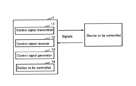
[0010] [FIG. 1] FIG. 1 is a block diagram showing the configuration of an
exemplary control
device of the present invention.
[FIG. 2] FIG. 2 is a flow chart showing an exemplary process of the control
device of
the present invention.
[FIG. 31 FIG. 3 is a diagram for explaining an example of signal generation
and control
in the present invention.
[FIG. 41 FIG. 4 is a diagram for explaining another example of signal
generation and
control in the present invention.
[FIG. 5] FIG. 5 is a block diagram showing the configuration of an exemplary
control
device system of the present invention.
Date Regue/Date Received 2023-04-04
CA 031.10470 2021-02-23
3
[FIG. 6] FIG. 6 is a block diagram showing the configuration of an exemplary
runway
flash lighting device control system of the present invention.
DESCRIPTION OF EMBODIMENTS
[0011] The runway flash lighting device control system of the present
invention includes: a
flash lighting control device; and a flash lighting device, wherein the flash
lighting control
device and the flash lighting device transmit and receive control signals to
and from each other
by wired signals, the flash lighting control device includes the first control
device according to
the present invention, the flash lighting device includes the second control
device according to
the present invention, flashing of the flash lighting device is controlled by
the control signal from
__ the flash lighting control device, and control of the flash lighting
control device is controlled by
the control signal from the flash lighting device.
[0012] The first control method of the present invention includes: a control
signal transmitting
step; a control signal receiving step; a control signal generating step; and a
control signal
controlling step, wherein the control signal transmitting step transmits a
signal to a device to be
controlled, the control signal receiving step receives a signal from the
device to be controlled, the
control signal generating step generates a control signal of 2 bytes or more
in one transmission
cycle, in the control signal, an address is assigned to each byte, and each
address is ON/OFF
switchable, the address of the control signal of 2 bytes or more includes a
main signal address
and a collation signal address associated with the main signal address, in a
case where the main
signal address and the collation signal address are the same signal, the
control signal controlling
step turns the collation signal address ON when the main signal address is ON
and turns the
collation signal address OFF when the main signal address is OFF, and in a
case where the main
signal address and the collation signal address are inverted, the control
signal controlling step
turns the collation signal address OFF when the main signal address is ON and
turns the
collation signal address ON when the main signal address is OFF.
[0013] The second control method of the present invention includes: a control
signal transmitting
step; a control signal receiving step; a control signal generating step; and a
control signal
controlling step, wherein the control signal transmitting step transmits a
signal to a device to be
controlled, the control signal receiving step receives a signal from the
device to be controlled, the
control signal generating step generates a control signal of 2 bytes or more
in one transmission
cycle, in the control signal, an address is assigned to each byte, and each
address is ON/OFF
switchable, and when a specific address is turned ON in a nth control signal,
the control signal
controlling step turns ON the same address as the specific address turned ON
in the nth control
signal at least twice consecutively even in the nth and subsequent control
signals.
Date Recue/Date Received 2021-02-23
CA 031.10470 2021-02-23
4
[0014] The program of the present invention is a program that can execute the
method
according to the present invention on a computer.
[0015] The computer-readable recording medium of the present invention is a
computer-
readable recording medium recorded with the program according to the present
invention.
[0016] The application of the present invention is not particularly limited.
The present
invention is applicable, for example, to a flash lighting control device, a
flash lighting device,
and a runway flash lighting device control system as described above. In
addition, the present
invention is also applicable to a system for transmitting and receiving wired
control signals such
as traffic signals, train signals, and the like.
[0017] Next, the embodiments of the present invention will be described with
reference to
FIGs. 1 to 6. The present invention is not limited or restricted by the
following embodiments by
any means. In FIGs. 1 to 6, identical parts are indicated with identical
reference signs. Regarding
the descriptions of the embodiments, reference can be made to one another.
Furthermore, for
convenience in explanation, the structure of each component may be
appropriately simplified,
and the size, the ratio, and the like of components may be schematically shown
and different
from actual ones.
[0018] [First embodiment]
The present embodiment relates to the first control device of the present
invention. FIG.
1 is a block diagram showing the configuration of an exemplary control device
according to the
present embodiment. As shown in FIG. 1, a control device 1 includes a control
signal transmitter
11, a control signal receiver 12, a control signal generator 13, and a control
signal controller 14.
[0019] The control signal transmitter 11 transmits signals to a device to be
controlled. The
control signal transmitter 11 is only required to be capable of transmitting
signals to the device to
be controlled, and examples thereof include a central processing unit (CPU), a
microprocessor,
and a microcontroller (microcomputer).
[0020] The control signal receiver 12 receives signals from a device to be
controlled. The
control signal receiver 12 is only required to be capable of receiving signals
from the device to
be controlled, and examples thereof include a CPU, a microprocessor, and a
microcomputer.
[0021] The control signal generator 13 generates control signals of 2 bytes or
more in one
transmission cycle. In the control signal, an address is assigned to each
byte, and each address is
ON/OFF switchable. The address of the control signal of 2 bytes or more
includes a main signal
address and a collation signal address associated with the main signal
address. The control signal
generator 13 is only required to be capable of generating the control signals,
and examples
thereof include a CPU, a microprocessor, and a microcomputer.
Date Recue/Date Received 2021-02-23
CA 031.10470 2021-02-23
[0022] In the case where the main signal address and the collation signal
address are the same
signal, the control signal controller 14 turns the collation signal address ON
when the main
signal address is ON and turns the collation signal address OFF when the main
signal address is
OFF. In the case where the main signal address and the collation signal
address are inverted, the
5 control signal controller 14 turns the collation signal address OFF when
the main signal address
is ON and turns the collation signal address ON when the main signal address
is OFF. The
control signal controller 14 is only required to be capable of controlling the
control signals, and
examples thereof include a CPU, a microprocessor, and a microcomputer.
[0023] Next, an example of the treatment (the first control method of the
present invention) in
the present device 1 will be described using the block diagram of FIG. 1 and
the flowchart of
FIG. 2. It is to be noted, however, that there is no limitation on the order
of performing the steps
as long as the first control method of the present invention includes a
control signal generating
step and a control signal controlling step and a control signal transmitting
step corresponding
thereto, which are performed at least once in this order. A plurality of steps
may be
simultaneously performed if it is possible. The number of times of performing
each step is not
particularly limited, and each step may be performed once or may be performed
a plurality of
times (two or more times).
[0024] In the example shown in FIG. 2, first, a control signal of 2 bytes or
more is generated in
one transmission cycle (Si). In the control signal, an address is assigned to
each byte, and each
address is ON/OFF switchable. The address of the control signal of 2 bytes or
more includes a
main signal address and a collation signal address associated with the main
signal address.
[0025] Control signal generation in the present embodiment will be described
using FIG. 3. In
the present embodiment, the control signal is only required to be 2 bytes or
more in one
transmission period. In the case of the control device for the flash lighting
control device of the
runway flash lighting device control system, for example, the control signal
may be a control
signal of 256 bytes in a transmission period (clock frequency) of 0.5 seconds,
which is a flash
lighting period, as shown in FIG. 3. In the control signal, addresses (1, 2,
3,..., 255, 256) are
assigned to respective bytes, and the addresses are ON/OFF switchable. In the
example shown in
FIG. 3, when a voltage of ¨10V is applied to a specified address, the
specified address is turned
ON (=1), and when no voltage (0V) is applied to a specific address, the
specific address is turned
OFF ()). The address of the control signal includes a main signal address
corresponding to each
transmission content and a collation signal address associated with the main
signal address. For
example, the address 5 is a main signal address for ordering light emission of
the flash lighting
device, and the address 13 is a collation signal address associated with the
main signal address 5.
Date Recue/Date Received 2021-02-23
CA 031.10470 2021-02-23
6
Similarly, for example, the address 6 is a main signal address for ordering
flash lighting at a low
light intensity, the address 14 is a collation signal address associated with
the main signal address
6, the address 7 is a main signal address for ordering flash lighting at a
medium light intensity,
the address 15 is a collation signal address associated with the main signal
address 7, the address
8 is a main signal address for ordering activation of the heater, and the
address 16 is a collation
signal address associated with the address 8.
[0026] Next, in the case where the main signal address and the collation
signal address are the
same signal, the collation signal address is turned ON when the main signal
address is ON and
the collation signal address is turned OFF when the main signal address is
OFF, and in the case
where the main signal address and the collation signal address are inverted,
the collation signal
address is turned OFF when the main signal address is ON and the collation
signal address is
turned ON when the main signal address is OFF (S2). In the example shown in
FIG. 3, the main
signal address and the collation signal address are the same signal such that
when the main signal
address 5 for ordering light emission of the flash lighting device is ON, the
collation signal
address 13 associated therewith is also turned ON, and when the other main
signal addresses are
OFF, the collation signal addresses associated therewith are also turned OFF.
Instead of the
example shown in FIG. 3, the main signal address and the collation signal
address may be
inverted such that when the main signal address 5 for ordering light emission
of the flash lighting
device is ON, the collation signal address 13 associated therewith is turned
OFF, and when the
other main signal addresses are OFF, the collation signal addresses associated
therewith are
turned ON.
[0027] Next, a signal is transmitted to a flash lighting device, which is a
device to be controlled
(S3). Thereby, the flash lighting device is ordered to emit light.
[0028] Next, a signal from the flash lighting device, which is the device to
be controlled, is
received (S4).
[0029] The present embodiment can improve the detection accuracy of the
control signal by
using two addresses, i.e., the main signal address and the collation signal
address, thereby
achieving a control device and a control method that can perform signal
processing without
being affected by the noise.
[0030] In addition, the present embodiment allows a long-distance transmission
of a control
signal and allows both of ordinary electric wires and optical cables to be
used for transmission of
a control signal, thereby achieving an inexpensive device configuration.
[0031] [Second embodiment]
The present embodiment relates to the second control device of the present
invention.
Date Recue/Date Received 2021-02-23
CA 031.10470 2021-02-23
7
The configuration of an exemplary control device 1 of the present embodiment
is the same as
that of the first control device of the first embodiment shown in FIG. 1. The
control device 1
includes a control signal transmitter 11, a control signal receiver 12, a
control signal generator
13, and a control signal controller 14.
[0032] The control signal transmitter 11 and the control signal receiver 12
are the same as those
in the first control device of the first embodiment.
[0033] The control signal generator 13 generates a control signal of 2 bytes
or more in one
transmission cycle. In the control signal, an address is assigned to each
byte, and each address is
ON/OFF switchable. As in the first embodiment, the control signal generator 13
is only required
to be capable of generating a control signal, and examples thereof include a
CPU, a
microprocessor, and a microcomputer.
[0034] When a specific address is turned ON in the nth control signal, the
control signal
controller 14 turns ON the same address as the specific address turned ON in
the nth control
signal at least twice consecutively even in the nth and subsequent control
signals. The control
signal controller 14 is only required to be capable of controlling a control
signal, and examples
thereof include a CPU, a microprocessor, and a microcomputer.
[0035] Next, an example of the treatment (the second control method of the
present invention)
in the present device 1 will be described using the block diagram of FIG. 1
and the flowchart of
FIG, 2. It is to be noted, however, that there is no limitation on the order
of performing the steps
as long as the second control method of the present invention includes a
control signal generating
step and a control signal controlling step and a control signal transmitting
step corresponding
thereto, which are performed at least once in this order. A plurality of steps
may be
simultaneously performed if it is possible. The number of times of performing
each step is not
particularly limited, and each step may be performed once or may be performed
a plurality of
times (two or more times).
[0036] In the example shown in FIG. 2, first, a control signal of 2 bytes or
more is generated in
one transmission cycle (Si). In the control signal, an address is assigned to
each byte, and each
address is ON/OFF switchable.
[0037] Control signal generation in the present embodiment will be described
using FIG. 4. In
the present embodiment, the control signal is only required to be 2 bytes or
more in one
transmission period. In the case of the control device for the flash lighting
device of the runway
flash lighting device control system, for example, the control signal may be a
control signal of
256 bytes in a transmission period (clock frequency) of 0.5 seconds, which is
a flash lighting
period, as shown in FIG. 4. In the control signal, addresses (1, 2, 255,
256) are assigned to
Date Recue/Date Received 2021-02-23
CA 031.10470 2021-02-23
8
respective bytes, and the addresses are ON/OFF switchable. In the example
shown in FIG. 4,
when a voltage of ¨10V is applied to a specified address, the specified
address is turned ON
(=I), and when no voltage (0V) is applied to a specific address, the specific
address is turned
OFF ()).
[0038] Next, when a specific address is turned ON in a nth control signal, the
control signal
controller turns ON the same address as the specific address turned ON in the
nth control signal
at least twice consecutively even in the nth and subsequent control signals
(S2). In the example
shown in FIG. 4, since the address 33 is turned ON in the first control
signal, the same address
33 as the address 33 turned on in the first control signal is turned ON three
times consecutively
in the first and subsequent control signals. For example, a specific
transmission content is
allocated to the each of the addresses 1 to 256 such that the address 33 is an
address for notifying
an abnormality in the flash lighting device, the address 34 is an address for
notifying the
abnormality of the power supply, the address 35 is an address for notifying
the two-circuit
interruption of the flash lighting source such as an LED, the address 161 is
an address for
notifying the activation of the heater, the address 201 is an address for
ordering the life-and-
death monitoring, and the like. The number of times of consecutively turns a
specific address ON
may be two or four or more times, and is preferably three times.
[0039] Next, a signal is transmitted to a flash lighting control device, which
is a device to be
controlled (S3). Thereby, the flash lighting control device detects an anomaly
in the flash lighting
device.
[0040] Next, a signal from the flash lighting control device, which is the
device to be
controlled, is received (S4).
[0041] The present embodiment can provide a control device and a control
method that can
perform signal processing without being affected by the noise by turning ON
the same address as
the specific address at least twice consecutively in a plurality of times of
control signals.
[0042] In addition, as in the first embodiment, the present embodiment allows
a long-distance
transmission of a control signal and allows both of ordinary electric wires
and optical cables to
be used for transmission of a control signal, thereby achieving an inexpensive
device
configuration.
[0043] [Third embodiment]
The present embodiment relates to the control device system of the present
invention.
FIG. 5 is a block diagram showing the configuration of an exemplary control
device system
according to the present embodiment. As shown in FIG. 5, a control device
system 2 includes
two control devices la and lb. One control device la of the two control
devices is the first
Date Recue/Date Received 2021-02-23
CA 031.10470 2021-02-23
9
control device of the present invention. The other control device lb of the
two control devices is
the second control device of the present invention. The two control devices la
and lb transmit
and receive control signals to and from each other by wired signals.
[0044] Next, the control device system 2 of the present embodiment will be
described using
FIG. 6 with reference to a runway flash lighting device control system. As
shown in FIG. 6, the
runway flash lighting device control system 2 includes a flash lighting
control device la, which
is the first control device of the present invention, and a flash lighting
device lb, which is the
second control device of the present invention. The flash lighting control
device la constitutes a
controller 20 together with a sequencer (computer) 21 connected thereto.
[0045] The present system 2 has a pair of communication wires, one of which is
an input wire
for transmitting a control signal from the controller 20 (flash lighting
control device la) to the
flash lighting device lb, and the other of which is an output wire for
performing feed back of
information from the flash lighting device lb to the controller 20 (flash
lighting control device
la). One of the pair of communication wires may be referred to as a (+) line,
and the other may
be referred to as a line. The flash lighting control device la and flash
lighting device lb
transmit and receive control signals to and from each other by wired signals,
flashing of the flash
lighting device lb is controlled by the control signal from the flash lighting
control device la,
and control of the flash lighting control device la is controlled by the
control signal from the
flash lighting device lb.
[0046] The present embodiment can provide a control device system that can
perform signal
processing without being affected by the noise.
[0047] In addition, the present embodiment allows a long-distance transmission
of a control
signal and allows both of ordinary electric wires and optical cables to be
used for transmission of
a control signal, thereby achieving an inexpensive system configuration.
[0048] [Fourth embodiment]
The program of the present embodiment is a program that can execute the
control
method of the first embodiment or the second embodiment on a computer. The
program of the
present embodiment may be recorded on, for example, a computer-readable
recording medium.
The recording medium is not particularly limited, and examples thereof include
a read-only
memory (ROM), a hard disk (HD), an optical disk, and a floppy disk (FD).
[0049] While the present invention has been described above with reference to
illustrative
example embodiments, the present invention is by no means limited thereto.
Various changes and
variations that may become apparent to those skilled in the art may be made in
the configuration
and specifics of the present invention without departing from the scope of the
present invention.
Date Recue/Date Received 2021-02-23
88044234
Industrial Applicability
[0050] The present invention can provide a control device that can perform
signal processing
without being affected by the noise and a control device system using the
same.
Reference Signs List
5 [0051]
1, la, lb: control device
2: control device system, runway flash lighting device control system
11: control signal transmitter
12: control signal receiver
10 13: control signal generator
14: control signal controller
Date Recue/Date Received 2022-06-09