Note : Les descriptions sont présentées dans la langue officielle dans laquelle elles ont été soumises.
BYPASS SWITCH FOR IN-LINE POWER STEAL
Background
The present disclosure pertains to thermostats and
particularly to various kinds of power supply arrangements for
thermostats.
Summary
The disclosure reveals a power supply unit for use with
thermostats or other like devices. The power supply unit may
keep electromagnetic interference emissions and harmonics at a
minimum. A unit may have enough power for triggering a switch
at about a cross over point of a waveform of input power to the
unit. Power for triggering may come from a storage source.
Power for the storage source may be provided with power stealing
which require switching transistors which can generate
emissions. In-line thermostats using MOSFETS power steal may do
the power steal during an ON state (triac, relay or silicon
controlled rectifier activated). Gate signals to the
transistors may be especially shaped to keep emissions from
transistor switching at a minimum. All that may be needed,
during an OFF state as a bypass, is a high voltage controllable
switch. The need may be achieved using high voltage MOSFETS.
Brief Description of the Drawing
Figure la is a block diagram of a thermostat circuit;
Figure lb is a diagram of a power supply unit having a
layout divided into several areas incorporating an off state
area, an always active area and an on state area;
Figure 2a is a diagram of a positive bypass switch;
Figure 2b is a diagram of a positive protect circuit
connected to the positive bypass switch;
1
Date Regue/Date Received 2022-12-05
Figure 3a is a diagram of a negative bypass switch;
Figure 3b is a diagram of a negative protect circuit
connected to the negative bypass switch;
Figure 4 is a diagram of a circuit showing power steal
switching MOSFETs;
Figure 5 is a diagram of a circuit showing a large capacity
capacitor;
Figure 6 is a diagram of a DC-DC converter or linear
regulator circuit;
Figure 7 is a diagram of a half wave zero crossing detect
circuit;
Figure 8a and Figure 8b are diagrams of a MOSFET gate
signal shaping circuit;
Figure 9 is a diagram of a MOSFET reverse wave protection
circuit;
Figure 10 is a diagram of an SCR gate triggering signal
circuit;
Figure 11 is a diagram of an SCR circuit; and
Figure 12 is a diagram of a plug that may be used for
various connections external to the power supply unit.
Description
The present system and approach may incorporate one or more
processors, computers, controllers, user interfaces, wireless
and/or wire connections, and/or the like, in an implementation
described and/or shown herein.
This description may provide one or more illustrative and
specific examples or ways of implementing the present system and
approach. There may be numerous other examples or ways of
implementing the system and approach.
There may be a need for a new kind of bypass which is non-
current limited, inexpensive, small space, power dissipation
2
Date Regue/Date Received 2022-12-05
proportional to current consumption, audible noise free and
electromagnetic interference compliant.
Since in-line thermostats using MOSFETS (metal-oxide-
semiconductor field-effect transistors) power steal may already
do the power steal during the ON state (triac, relay or silicon
controlled rectifier (SCR) activated). All that may be needed,
during the OFF state as a bypass, is a high voltage controllable
switch. This may be achieved using high voltage MOSFETS.
The thermostats may relate to HVAC (heating, ventilation
and air conditioning) systems.
Using the same synchronization as for a MOSFET power steal,
one may synchronize the MOSFET switch. For an energy hungry
application, the peak current through the switch can became very
high since the power steal is half wave only. So, a second
switch with small modification to the synchronization circuit
may be added to make a full wave switch and reduce harmonics.
The present approach may be used with an in-line controller
doing MOSFET power steal like the line volt thermostat. It may
allow a circuit to be universal for virtually all thermostats,
and that has characteristics such as being non-current limited,
inexpensive, situated in a small space, having power dissipation
proportional to current consumption, and being audible noise
free and electromagnetic interference compliant. The present
approach may use one or more switches in a power steal circuit
for an in-line thermostat
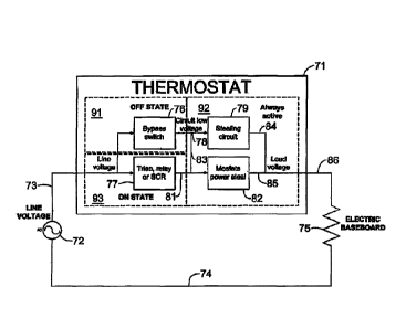
Figure la is a block diagram of a thermostat circuit 71
discussed herein. An AC (alternating current) line voltage may
be provided by power supply 72 on lines 73 and 74 to thermostat
71 and electric baseboard 75. Line voltage on line 73 may go to
a bypass switch 76 and triac, relay or SCR 77. Circuit low
voltage may go along line 78 to stealing circuit 79. A
connection may go from triac, relay or SCR 77 to a MOSFETs power
3
Date Regue/Date Received 2022-12-05
steal 82 along line 81. Lines 78 and 81 may be connected by a
line 83. A load voltage may connect stealing circuit 79 and
MOSFETs power steal 82 along lines 84 and 85 via line 86 to
electric baseboard 75. Areas 91, 92 and 93 indicate off state,
always active and on state, respectively.
Figure lb is a diagram of a power supply unit 11 having a
layout divided into three areas incorporating an off state area
12, an always active area 13 and an on state area 14.
A positive bypass switch 15 in area 12 may have an input
from a line 16 (2). Also in area 15 is a negative bypass switch
17. Line 16 may go to negative bypass switch 17. An AGND line
21 may be an input to switch 17.
Power steal switching MOSFETs 18 in area 13 may have an
input from a line 19 (1) and be connected to an AGND (ground)
line 21. A line 22 may go from negative bypass switch to power
steal switching MOSFETs 18.
An energy storage 23 in area 13 may receive an input of
Vrect (stolen energy) on line 24 from positive bypass switch 15
and an RS1G input on line 24 from power steal switching MOSFETs
18. An output Vrect on line 24 may go from energy storage 23 to
a DC-DC (direct current) converter or linear regulator 25 of
area 13. An output Vcc (3Vdc) on a line 26 may go outside of
unit 11 to a processor and circuits 27. Vrect on line 24 may go
to a backlight circuit 28 outside of unit 11. Vrect on line 24
may also go to negative bypass switch 17.
A half wave ZC (zero crossing) detect 31 in area 13 may
have an input connected to line 16 and an input connected to
Vrect on line 24. Detect 31 may output a D latch positive
signal on a line 32, a D latch negative signal on a line 33, and
a crossing signal on a line 34. The signals on lines 32, 33 and
34 may go to a MOSFET gate signal shaping circuit 35 in area 13.
4
Date Regue/Date Received 2022-12-05
A MOSFET reverse wave protection circuit 36 in area 13 may
have an input of Vrect on line 24 and of line 19 (1) of AC in.
A protect signal on a line 37 may go from protection circuit 36
to shaping circuit 35. A Vsync signal on a line 38 may go from
shaping circuit 35 to positive bypass switch 15 and to negative
bypass switch 17. A Vg signal may be on a line 39 and may go to
power steal switching MOSFETs 18.
An SCR gate triggering signal circuit 41 of area 14 may
have inputs of Vrect on line 24, line 16 (2) of AC in and a CPU
(computer) drive signal on a line 42. Circuit 41 may provide a
gate signal Vgm+ on a line 43 and a gate signal Vgm- on a line
44 to an SCR circuit 45 of area 14. Line 16 (2) of AC in may be
an input to SCR circuit 45. An AC out on a line 46 may be
provided by circuit 45.
Figure 2a is a diagram of positive bypass switch 15.
Switch 15 may be connected to a positive protect circuit 51 as
shown in a diagram of Figure 2b. A Vdp signal may go on a line
53 from switch 15 to circuit 51.
Figure 3a is a diagram of negative bypass switch 17.
Switch 17 may be connected to a negative protect circuit 52 as
shown in a diagram of Figure 3b. A Vdn signal may go on a line
58 from switch 17 to circuit 52. An over current terminal in
circuit 51 may be connected via a line 57 with an over current
terminal in circuit 52.
Figure 4 is a diagram of circuit 18 showing power steal
switching MOSFETs 61 and 62. Figure 5 is a diagram of circuit
23 showing a large capacity (e.g., 820 microfarads) capacitor
63. Figure 6 is a diagram of a DC-DC converter or linear
regulator circuit 25.
Figure V is a diagram of a half wave zero crossing detect
circuit 31. Figure 8a and Figure 8b are diagrams of MOSFET gate
signal shaping circuit 35. Lines 21, 24, 34, 37 and 65 connect
5
Date Regue/Date Received 2022-12-05
the diagrams of Figures 8a and 8b to show the whole circuit 35.
Figure 9 is a diagram of MOSFET reverse wave protection circuit
36.
Figure 10 is a diagram of SCR gate triggering signal
circuit 41, which provides trigger signals Vgm+ and Vgm- on
lines 43 and 44 to SCR circuit 45 shown in a diagram of Figure
11.
Figure 12 is a diagram of a plug 66 that may be used for
various connections external to unit 11.
To recap, an in-line thermostat power system may
incorporate a bypass switch, a power stealing circuit connected
to the bypass switch, an energy storage circuit connected to the
power stealing circuit, an SCR interface circuit connected to
the energy storage circuit, and an SCR circuit connected to the
SCR interface circuit. The bypass switch may be a controllable
switch for line voltage.
The line voltage controllable switch may incorporate a
positive bypass switch and a negative bypass switch. The
positive bypass switch may incorporate one or more line voltage
MOSFETs. The negative bypass switch may incorporate one or more
line voltage MOSFETs.
The positive bypass switch may incorporate a positive
protect circuit. The negative bypass switch may incorporate a
negative protect circuit.
The system may further incorporate a half wave zero
crossing detection circuit connected to the energy storage
circuit, and a gate signal shaping circuit connected to the half
wave zero crossing detection circuit, the bypass switch, and the
power stealing circuit. The power stealing circuit may
incorporate one or more switching MOSFETs. The gate signal
shaping circuit may provide a gate signal that results in a soft
6
Date Regue/Date Received 2022-12-05
transition of turning on and off of the one or more MOSFETs of
the power stealing circuit.
The SCR interface circuit may have a first input connected
to an output of the energy storage circuit, a second input
connectable to a line voltage, a third input connectable to a
control signal source, and an output of gate signals. The SCR
circuit may have a first input for gate signals from the SCR
interface circuit, a second input connectable to a line voltage,
and an output of a controlled line voltage.
The system may further incorporate a thermostat having a
temperature sensor, a temperature setting adjuster, and a
processor connected to the temperature sensor and a temperature
setting adjuster. The processor may incorporate the control
signal source that provides a signal to the SCR interface
circuit which in turn outputs the gate signals to the SCR
circuit, with a goal to bring a temperature indication from the
temperature sensor and a temperature setting of the temperature
setting adjuster to a same value.
The system may further incorporate a heater having
terminals connected to a line voltage and an output of the SCR
circuit. The temperature sensor may be situated in a space that
contains the heater. The gate signals to the SCR may result in
the output of the SCR circuit to control heat from the heater to
achieve the goal to bring the temperature indication from the
temperature sensor and the temperature setting of the
temperature setting adjuster to a same value.
A thermostatic power supply mechanism may incorporate a
first terminal for connection of a power source; a bypass switch
having an input connected to the first terminal; an SCR circuit
having a first connection connected to the first terminal, an
input for a control signal, and a second connection connectable
to a load; a second terminal for connection to a load; a
7
Date Regue/Date Received 2022-12-05
stealing circuit having an input connected to an output of the
bypass switch, and an output connected to the second terminal;
and a power steal module having an input connected to the output
of the SCR circuit and an output connected to the second
terminal.
The bypass switch may incorporate one or more MOSFETs that
are switched. The power steal module may incorporate one or
more MOSFETs that are switched to steal power. The stealing
circuit may have an energy storage unit. Stolen power may go to
the energy storage.
The energy storage cell may incorporate one or more super
capacitors.
The bypass switch may have circuitry that incorporates a
positive bypass switching MOSFET, and a negative bypass
switching MOSFET.
The mechanism may further incorporate a MOSFET gate signal
shaper that provides a gate signal to the power steal module
that softens a transition of turning on or off of the one or
more MOSFETs.
The mechanism may further incorporate an SCR control signal
circuit having an output that provides the control signal to the
input of the SCR circuit. The control signal provided to the
input of the SCR circuit may result in making power available or
not available at the second connection of the SCR circuit. The
second connection of the SCR circuit may be connected to the
load. The load may be a heater.
A power supply unit for a thermostat and electric heater
may incorporate a bypass switch circuit having an input
connectable to a first line voltage, a power steal device having
an input connectable to an output of the bypass switch circuit,
an energy storage having an input connected to an output of the
power steal device, an SCR gate signal circuit having an input
8
Date Regue/Date Received 2022-12-05
connected to an output of the energy storage, and an SCR circuit
having an input from an output of the SCR gate signal circuit
and an input connectable to a second line voltage, and having an
output for providing a controlled second line voltage. The
bypass switch circuit may have one or more MOSFET switches.
Also, the power steal device may have one or more MOSFET
switches.
The unit may further incorporate a linear regulator
connected to the output of the energy storage.
The unit may further incorporate a zero crossing detector
having an input connectable to the second line voltage.
The unit may further incorporate a FET gate signal shaping
circuit having an input for receiving zero crossing information
from the zero crossing detector and having an output for
providing a sync signal to the bypass switch circuit.
The unit may further incorporate a reverse wave protection
circuit having an input connected to the first line voltage, a
second input connected to the output of the energy storage, and
having an output for providing a protect signal to the FET gate
signal shaping circuit.
U.S. Patent Application No. 13/868,754, filed April 23,
2013, and entitled "Triac or Bypass Circuit and MOSFET Power
Steal Combination".
In the present specification, some of the matter may be of
a hypothetical or prophetic nature although stated in another
manner or tense.
Although the present system and/or approach has been
described with respect to at least one illustrative example,
many variations and modifications will become apparent to those
skilled in the art upon reading the specification. It is
therefore the intention that the appended claims be interpreted
9
Date Regue/Date Received 2022-12-05
as broadly as possible in view of the related art to include all
such variations and modifications.
Date Regue/Date Received 2022-12-05