Note : Les descriptions sont présentées dans la langue officielle dans laquelle elles ont été soumises.
1
DESCRIPTION
Title of Invention:
METHOD FOR MANUFACTURING ELECTRODE, AND ELECTRODE
Technical Field
[0001] The present invention relates to a method for
producing an electrode, and an electrode produced by the
method for producing an electrode.
Background Art
[0002] A water electrolysis technique is low cost,
suitable for enlargement of scale, and therefore is a
predominant technique for hydrogen production. Among the
elements which are used for water electrolysis, many of
anodes have an oxygen evolution overpotential of exceeding
0.3 V under actual operation conditions. It can be said
that there is room for significant improvement in the oxygen
evolution overpotential as compared to the fact that hydrogen
evolution and chlorine evolution overpotentials utilized in
current electrolysis industry are around 0.1 V.
[0003] For example, as an alkaline water electrolysis
anode, an electrode formed by a nickel alloy or the like
that is stable in a high-concentration alkali aqueous
solution, an electrode using this electrode as an
electrically conductive substrate and having a catalyst
layer or the like provided on a surface of the electrode, or
the like is used.
[0004] To make an electrically conductive substrate
composed of a nickel alloy into an electrode, an etching
treatment for example is performed using an etchant in order
to remove a components such as an organic material adhering
to the surface or to improve adhesiveness with a catalyst
layer. Specifically, a method of immersing an electrically
conductive substrate composed of a nickel alloy in boiling
hydrochloric acid to perform an etching treatment is known
CA 03224135 2023 12 22
2
(Patent Literatures 1 and 2).
Citation List
Patent Literature
[0005]Patent Literature 1: Japanese Patent Laid-Open No.
2017-190476
Patent Literature 2: International Publication No. WO
2018/047961
Summary of Invention
Technical Problem
[0006] However, oxygen evolution reaction (OER)
activity of an electrode obtained by an etching treatment
according to any of the methods disclosed in Patent
Literatures 1 and 2, and the like is not so high, and there
has been room for further improvements.
[0007] The present invention has been completed in view
of such problems of the conventional techniques, and an
object of the present invention is to provide a simple method
for producing an electrode having improved oxygen evolution
reaction (OER) activity without a need for catalyst coating.
In addition, another object of the present invention is to
provide an electrode produced by the above-described
production method and suitable as an oxygen evolution anode
or the like.
Solution to Problem
[0008] That is, according to the present invention, a
method for producing an electrode, described below, is
provided.
[1] A method for producing an electrode, including: a step
of subjecting an electrically conductive substrate composed
of a nickel alloy containing 30 to 70% by mass of Ni and 30
to 70% by mass of Fe, provided that Ni + Fi = 100% by mass,
to a thermal treatment; and a step of etching the thermally
treated electrically conductive substrate with an etchant
CA 03224135 2023 12 22
3
containing at least any acid of an organic acid and a weak
inorganic acid.
[2] The method for producing an electrode according to [1],
wherein the organic acid is acetic acid, and the weak
inorganic acid is boric acid.
[3] The method for producing an electrode according to [1]
or [2], further including a step of subjecting a surface of
the electrically conductive substrate before being subjected
to the thermal treatment to blasting.
[4] The method for producing an electrode according to any
one of [1] to [3], wherein the nickel alloy contains 40 to
60% by mass of Ni and 40 to 60% by mass of Fe, provided that
Ni + Fe = 100% by mass.
[5] The method for producing an electrode according to any
one of [1] to [4], further including a step of providing a
catalyst layer on the surface of the etched electrically
conductive substrate.
[6] The method for producing an electrode according to [5],
further including a step of providing an intermediate layer
between the surface of the etched electrically conductive
substrate and the catalyst layer.
[7] The method for producing an electrolysis electrode
according to any one of [1] to [6], wherein the electrode is
an oxygen evolution anode.
[0009] In addition, according to the present invention,
an electrode described below is provided.
[8] An electrode produced by the production method according
to any one of [1] to [7].
Advantageous Effects of Invention
[0010] The present invention can provide a simple method
for producing an electrode having improved oxygen evolution
reaction (0ER) activity without a need for catalyst coating.
In addition, the present invention can provide an electrode
produced by the above-described production method and
suitable as an oxygen evolution anode or the like.
CA 03224135 2023- 12- 22
4
Brief Description of Drawings
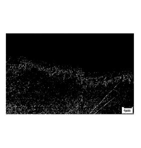
[0011][Figure 1A] Figure 1A is an electron micrograph of a
surface of an electrode produced in Example 1.
[Figure 1B] Figure 1B is an electron micrograph of a section
of the electrode produced in Example 1.
[Figure 2A] Figure 2A is an electron micrograph of a surface
of an electrode produced in Example 2.
[Figure 2B] Figure 2B is an electron micrograph of a section
of the electrode produced in Example 2.
[Figure 3A] Figure 3A is an electron micrograph of a surface
of an electrode produced in Comparative Example 2.
[Figure 3B] Figure 3B is an electron micrograph of a section
of the electrode produced in Comparative Example 2.
[Figure 4A] Figure 4A is an electron micrograph of a surface
of an electrode produced in Comparative Example 8.
[Figure 4B] Figure 4B is an electron micrograph of a section
of the electrode produced in Comparative Example 8.
[Figure 5] Figure 5 is an electron micrograph of a section
of an electrode produced in Comparative Example 5.
Description of Embodiments
[0012]<Method for Producing Electrode>
Hereinafter, embodiments of the present invention will
be described, but the present invention is not limited to
the following embodiments.
A method for producing an
electrode of the present invention (hereinafter, also simply
referred to as "production method (of the present
invention)") includes a step (thermal treatment step) of
subjecting an electrically conductive substrate composed of
a nickel alloy to a thermal treatment; and a step (etching
step) of etching the thermally treated electrically
conductive substrate with an etchant. The nickel alloy that
forms the electrically conductive substrate contains 30 to
70% by mass of Ni and 30 to 70% by mass of Fe (provided that
Ni + Fe = 100% by mass). The etchant contains at least any
CA 03224135 2023- 12- 22
5
acid of an organic acid and a weak inorganic acid.
Hereinafter, details on the method for producing an electrode
of the present invention will be described.
[0013] (Thermal Treatment Step)
In the thermal treatment step, the electrically
conductive substrate composed of a nickel alloy is subjected
to a thermal treatment. When the electrically conductive
substrate is subjected to the thermal treatment, iron (Fe)
in the nickel alloy that forms the electrically conductive
substrate migrates to the surface of the electrically
conductive substrate and a surface layer containing Fe as
the main component is formed (Figure 5). The temperature of
the thermal treatment is preferably set to 500 to 600 C, more
preferably 520 to 580 C. By performing the thermal treatment
at the temperature within the above-described range, a
sufficient surface layer containing Fe as the main component
can be formed.
The time for the thermal treatment may
appropriately be set according to the shape, thickness, and
the like of the electrically conductive substrate.
Specifically, the time for the thermal treatment may be set
within about 1 to about 5 hours.
[0014]
The nickel alloy that forms the electrically
conductive substrate contains 30 to 70% by mass of nickel
(Ni) and 30 to 70% by mass of iron (Fe), preferably 40 to
60% by mass of Ni and 40 to 60% by mass of Fe. Provided
that the total of Ni and Fe is 100% by mass. In addition,
trace elements such as manganese (Mn), chromium (Cr), and
carbon (C) besides Ni and Fe may be contained in the nickel
alloy.
By using the electrically conductive substrate
formed with the nickel alloy in which the contents of Ni and
Fe are within the above-described ranges, an electrode having
improved oxygen evolution reaction (0ER) activity can be
produced.
Specific examples of the nickel alloy include
Invar 42 and Invar 36.
[0015]
The electrically conductive substrate is an
electric conductor that conducts electricity for
CA 03224135 2023- 12- 22
6
electrolysis. When an intermediate layer and a catalyst
layer are provided on a surface of the electrically
conductive substrate, the electrically conductive substrate
functions as a carrier that carries the intermediate layer
and the catalyst layer.
The whole of the electrically
conductive substrate may be formed with a nickel alloy, or
only the surface of the electrically conductive substrate
may be formed with a nickel alloy. The thickness of the
electrically conductive substrate is preferably 0.05 to 5
mm. The shape of the electrically conductive substrate is
preferably a shape having an opening for removing bubbles of
oxygen, hydrogen, and the like to be produced. For example,
an expanded mesh or a porous expanded mesh can be used as
the electrically conductive substrate.
When the
electrically conductive substrate has a shape having an
opening, the aperture ratio of the electrically conductive
substrate is preferably 10 to 95%.
[0016](Etching Step)
In the etching step, the thermally treated
electrically conductive substrate is etched with the etchant.
The etchant is a liquid (aqueous solution) containing at
least any acid of an organic acid and boric acid. When the
electrically conductive substrate after the thermal
treatment is etched with this etchant, at least a part of
the surface layer formed by the thermal treatment and
containing Fe as the main component can be removed. Thereby,
an electrode having a newly formed porous surface containing
Ni as the main component can be obtained (Figure 1B).
[0017]
The electrically conductive substrate can be
etched by, for example, immersing the thermally treated
electrically conductive substate in the etchant.
The
temperature of the etchant may be room temperature (20 C) or
higher, and is preferably set to 50 C or higher, and the
electrically conductive substrate is more preferably
immersed in the etchant which is boiling. When etching is
performed using the etchant at a predetermined temperature
CA 03224135 2023 12 22
7
or higher, thereby at least a part of the surface layer
containing Fe as the main component can be removed more
efficiently.
The time for immersing the electrically
conductive substrate in the etchant may appropriately be set
according to the shape, thickness, and the like of the
electrically conductive substrate. Specifically, the time
for immersing the electrically conductive substrate in the
etchant may be set within a range of about 0.1 to about 10
hours.
[0018]
The acid contained in the etchant is at least
any of an organic acid and a weak inorganic acid. When
etching is performed using the etchant containing any of
these acids, thereby at least a part of the surface layer
containing Fe as the main component can efficiently be
removed and an electrode having a newly formed porous surface
containing Ni as the main component can be obtained (Figure
1B). When etching is performed using an etchant containing
a so-called strong acid such as hydrochloric acid (HC1)
instead of an organic acid and a weak inorganic acid, a
porous surface cannot be formed (Figure 4B), and an electrode
having improved oxygen evolution reaction (0ER) activity
cannot be produced.
[0019]
As the organic acid, formic acid, acetic acid,
propionic acid, oxalic acid, citric acid, and the like can
be used. Among others, acetic acid is preferably used as
the organic acid. The weak inorganic acid is an inorganic
acid such that only some parts thereof are dissociated when
dissolved in water. The weak inorganic acid preferably has
a pKa of 2.0 to 10 in water at 25 C. Examples of the weak
inorganic acid include boric acid, phosphoric acid,
hydrofluoric acid, and hypochlorous acid.
Among others,
boric acid is preferably used as the weak inorganic acid.
The content (concentration) of the acid in the etchant may
appropriately be set according to the shape, thickness, and
the like of the electrically conductive substrate.
Specifically, the content (concentration) of the acid in the
CA 03224135 2023- 12- 22
8
etchant is preferably set to 5 to 75% by mass, more
preferably 7.5 to 60% by mass. In addition, the consumption
of the electrically conductive substrate by etching is
preferably set to about 1 to about 50 g/m2.
[0020] (Blast Step)
The production method of the present invention
preferably further includes a step (blast step) of subjecting
the surface of the electrically conductive substrate before
being subjected to the thermal treatment to blasting. When
the thermal treatment is performed after roughening the
surface of the electrically conductive substrate by blasting,
thereby in the case where an intermediate layer and a
catalyst layer are to be provided after the roughening, the
adhesiveness of these layers to the surface of the
electrically conductive substrate can be improved. Examples
of methods of subjecting the surface of the electrically
conductive substrate to blasting include a method of spraying
abrasive grains of an alumina powder or the like.
[0021] (Step of Forming Catalyst Layer)
The production method of the present invention
preferably further includes a step of providing a catalyst
layer on the surface of the etched electrically conductive
substrate. Examples of the catalyst that forms the catalyst
layer include platinum, a ruthenium oxide, an iridium oxide,
a rhodium oxide, and a palladium oxide corresponding to
various kinds of electrolysis. In the case of an oxygen
evolution electrode for which durability against evolved
oxygen, low pH, organic impurities, and the like are
particularly required, an iridium oxide is suitable.
Further, in order to improve adhesiveness with the
electrically conductive substrate and the intermediate layer
or durability against electrolysis, a titanium oxide, a
tantalum oxide, a niobium oxide, a tin oxide or the like is
preferably mixed in the catalyst. The catalyst layer can be
formed by a chemical solution deposition method, a sol-gel
method, a paste method, electrophoresis, a CVD method, a PVD
CA 03224135 2023- 12- 22
9
method, and the like. Among others, a chemical solution
deposition method disclosed in Japanese Patent Publication
No. 48-3954, Japanese Patent Publication No. 46-21884, and
the like, is preferable, wherein a coating solution
containing a metal compound to be the main component of a
catalyst layer is coated and dried, and then a heating and
calcining treatment is performed to produce an intended oxide
(catalyst) through thermal decomposition and thermal
synthesis reaction.
[0022]
Examples of the metal compound contained in the
coating solution include a metal alkoxide, a metal chloride,
and a metal nitrate. To the coating solution, hydrochloric
acid, nitric acid, oxalic acid, and as a chelating agent,
salicylic acid, 2-ethylhexanoic acid, acethyl acetone, EDTA,
ethanolamine, citric acid, and ethylene glycol and the like
as a stabilizer may be added. The coating solution is coated
on the surface of the electrically conductive substrate or
the intermediate layer by a coating method such as brush
coating, roller coating, spray coating, spin coating,
printing, or electrostatic coating, and then dried.
Subsequently, the heating and calcination treatment is
performed in an oxidative atmosphere such as air, and thereby
the catalyst layer can be formed.
The thickness of the
catalyst layer is preferably, for example, 0.01 to 100 m,
more preferably 0.1 to 10 m.
[0023] (Step of Forming Intermediate Layer)
The production method of the present invention
preferably further includes a step of providing an
intermediate layer between the surface of the etched
electrically conductive substrate and the catalyst layer.
When the intermediate layer is provided, thereby adhesion
force between the surface of the electrically conductive
substrate and the catalyst layer can further be enhanced.
The intermediate layer can be formed by the same method as
the above-described method for forming the catalyst layer.
Among others, the intermediate layer is preferably provided
CA 03224135 2023- 12- 22
10
between the surface of the etched electrically conductive
substrate and the catalyst layer by the above-described
chemical solution deposition method. The thickness of the
intermediate layer is preferably, for example, 0.01 to 100
m, more preferably 0.1 to 10 m.
[0024]<Electrode>
An electrode of the present invention is one produced
by the above-described method for producing an electrode.
That is, the electrode of the present invention is an
electrode obtained by subjecting the electrically conductive
substrate composed of a nickel alloy containing Ni and Fe in
a predetermined ratio to thermal treatment and then etching
the thermally treated electrically conductive substrate with
an etchant containing a particular acid. As described above,
if necessary, the intermediate layer and the catalyst layer
may be provided on the surface of the electrically conductive
substrate.
The electrode of the present invention is
obtained by the above-described production method, and
therefore oxygen evolution reaction (0ER) activity is
improved without a need for catalyst coating.
For this
reason, the electrode of the present invention is suitable
as, for example, an oxygen evolution anode.
Examples
[0025] Hereinafter, the present invention will
specifically be described based on Examples, but the present
invention is not limited to these Examples.
Note that
"parts" and "%" in Examples and Comparative Examples are on
a mass basis unless otherwise noted.
[0026]<Production (1) of Electrode>
(Example 1)
An electrically conductive substrate (thickness: 1 mm)
formed with a nickel alloy (Invar 42 (Ni 42%, Fe 58%)) was
prepared.
This electrically conductive substrate was
subjected to a blast treatment (0.3 MPa) with alumina
particles of 60 mesh and then subjected to a thermal
CA 03224135 2023 12 22
11
treatment at 53000 for 3 hours in an air environment. The
electrically conductive substrate was left standing to cool
and then subjected to an etching treatment by being immersed
in a 10% boiling boric acid aqueous solution for 20 minutes.
The etched electrically conductive substrate was left
standing to cool and then rinsed with water and dried to
obtain an electrode.
The consumption by the etching
treatment was 17.0 2.1 g/m2.
[0027] (Comparative Examples 1 to 5)
Each electrode was produced in the same manner as in
Example 1 described above except that an electrically
conductive substrate composed of each material shown in Table
1 and each treatment shown in Table 1 was performed. The
consumption (g/m2) by each etching treatment is shown in
Table 1.
[0028]<Measurement (1) of Oxygen Overpotential>
Electrolytic cells were prepared using the produced
electrodes as anodes and using nickel cathodes. The area of
each electrode was set to 4 cm2. Electrolysis was performed
using an electrolyte (30% KOH aqueous solution) at a current
density of 10 kA/m2 for 2 hours to measure oxygen
overpotential (mV). Measurement results are shown in Table
1.
[0029]
CA 03224135 2023- 12- 22
uJ
Lfl
Table 1
Electrically
Consumption (g/m2) Oxygen
Blast Thermal
conductive Etching
treatment by etching overpotential
treatment treatment
substrate
treatment (mV)
10% boiling boric acid aqueous
Example 1 Invar 42 Performed Performed solution
17.0 2.1 197
x 20 min
Comparative
Nickel Performed Not performed Not
performed 342
Example 1
Comparative
Invar 42 Performed Not performed Not
performed 257
Example 2
10% boiling acetic acid aqueous
Comparative
Invar 42 Performed Not performed solution
17.2 1.4 246
Example 3
x 20 min
10% acetic acid aqueous solution x
Comparative
Inver 42 Performed Not performed ultrasonic
waves 3.2 1.7 224
Example 4
x 30 min (room temperature)
Comparative
Invar 42 Performed Performed Not
performed N.D.
Example 5
13
[0030]<Production (2) of Electrode>
(Example 2)
An electrically conductive substrate (thickness: 1 mm)
formed with a nickel alloy (Invar 42 (Ni 42%, Fe 58%)) was
prepared.
This electrically conductive substrate was
subjected to a blast treatment (0.3 MPa) with alumina
particles of 60 mesh and then subjected to a thermal
treatment at 53000 for 3 hours in an air environment. The
electrically conductive substrate was left standing to cool
and then subjected to an etching treatment by being immersed
in a 10% boiling acetic acid aqueous solution for 20 minutes.
The etched electrically conductive substrate was left
standing to cool and then rinsed with water and dried to
obtain an electrode.
[0031] (Comparative Examples 6 and 7)
Each electrode was produced in the same manner as in
Example 2 described above except that an electrically
conductive substrate composed of a material (Permalloy 78
(Ni 78%, Fe 22%)) shown in Table 2 was used and each treatment
shown in Table 2 was performed.
[0032]<Measurement (2) of Oxygen Overpotential>
Oxygen overpotential (mV) was measured in the same
manner as in "Measurement (1) of Oxygen Overpotential"
described above. Measurement results are shown in Table 2
together with measurement results for the electrodes
produced in Comparative Examples 1 and 2.
[0033]
CA 03224135 2023- 12- 22
uJ
Lfl
Table 2
Electrically
Oxygen
Blast Thermal
conductive Etching treatment
overpotential
treatment treatment
substrate (mV)
10% boiling acetic acid
Example 2 Invar 42 Performed Performed
aqueous solution 201
x 20 min
Comparative
Nickel Performed Not performed Not
performed 342
Example 1
Comparative
Invar 42 Performed Not performed Not
performed 257
Example 2
Comparative
Permalloy 78 Performed Not performed Not
performed 280
Example 6
10% boiling acetic acid
Comparative
Permalloy 78 Performed Performed
aqueous solution 298
Example 7
x 20 min
15
[0034]<Production (3) of Electrode>
(Comparative Example 8)
An electrically conductive substrate (thickness: 1 mm)
formed with a nickel alloy (Invar 42 (Ni 42%, Fe 58%)) was
prepared.
This electrically conductive substrate was
subjected to a blast treatment (0.3 MPa) with alumina
particles of 60 mesh and then subjected to a thermal
treatment at 530 C for 3 hours in an air environment. The
electrically conductive substrate was left standing to cool
and then subjected to an etching treatment by being immersed
in a 10% boiling hydrochloric acid for 3 minutes. The etched
electrically conductive substrate was left standing to cool
and then rinsed with water and dried to obtain an electrode.
[0035]<Electron Micrographs of Electrodes>
Electron micrographs of the surfaces and sections of
respective electrodes produced in Examples 1 and 2,
Comparative Example 2, and Comparative Example 8 are shown
in Figures 1A to 4B. In addition, an electron micrograph of
a section of the electrode produced in Comparative Example
is shown in Figure 5.
[0036]
As shown in Figure 5, it is understood that when
the electrically conductive substrate is subjected to the
thermal treatment, thereby Fe in the nickel alloy (Invar 48)
migrates to form a surface layer.
As shown in Figures 1A to 2B, when the electrically
conductive substrate after the thermal treatment was
subjected to an etching treatment with a boric acid aqueous
solution or an acetic acid aqueous solution, thereby an
electrode on which a surface having a porous structure is
formed can be obtained. In contrast, as shown in Figures 3A
and 3B, by only subjecting the electrically conductive
substrate to a blast treatment, a surface having a porous
structure as shown in Figures 1A to 2B cannot be formed.
Further, as shown in Figures 4A and 4B, it is understood
that when the electrically conductive substrate after the
thermal treatment is subjected to an etching treatment with
CA 03224135 2023- 12- 22
16
hydrochloric acid, a surface having a porous structure as
shown in Figures lA and 2B cannot be formed.
Industrial Applicability
[0037]
An electrode produced by the production method
of the present invention is suitable as, for example, an
oxygen evolution anode.
CA 03224135 2023- 12- 22