Sélection de la langue

Search

Sommaire du brevet 2168172 

Énoncé de désistement de responsabilité concernant l'information provenant de tiers

Une partie des informations de ce site Web a été fournie par des sources externes. Le gouvernement du Canada n'assume aucune responsabilité concernant la précision, l'actualité ou la fiabilité des informations fournies par les sources externes. Les utilisateurs qui désirent employer cette information devraient consulter directement la source des informations. Le contenu fourni par les sources externes n'est pas assujetti aux exigences sur les langues officielles, la protection des renseignements personnels et l'accessibilité.

Disponibilité de l'Abrégé et des Revendications

L'apparition de différences dans le texte et l'image des Revendications et de l'Abrégé dépend du moment auquel le document est publié. Les textes des Revendications et de l'Abrégé sont affichés :

  • lorsque la demande peut être examinée par le public;
  • lorsque le brevet est émis (délivrance).
(12) Demande de brevet: (11) CA 2168172
(54) Titre français: METHODE DE FABRICATION DE GUIDES D'ONDES A MOULURES MULTISEGMENT
(54) Titre anglais: METHOD FOR FABRICATING MULTISEGMENT RIDGE WAVEGUIDES
Statut: Morte
Données bibliographiques
(51) Classification internationale des brevets (CIB):
  • H01L 21/302 (2006.01)
  • G02B 6/12 (2006.01)
  • G02B 6/136 (2006.01)
  • G03F 7/26 (2006.01)
  • H01L 21/306 (2006.01)
  • H01L 21/308 (2006.01)
(72) Inventeurs :
  • KUHN, EDGAR WOLFRAM (Allemagne)
(73) Titulaires :
  • ALCATEL N.V. (Pays-Bas (Royaume des))
(71) Demandeurs :
(74) Agent: ROBIC
(74) Co-agent:
(45) Délivré:
(22) Date de dépôt: 1996-01-26
(41) Mise à la disponibilité du public: 1996-07-29
Licence disponible: S.O.
(25) Langue des documents déposés: Anglais

Traité de coopération en matière de brevets (PCT): Non

(30) Données de priorité de la demande:
Numéro de la demande Pays / territoire Date
195 02 684.5 Allemagne 1995-01-28

Abrégés

Abrégé anglais


A process for fabricating multisegment ridge
waveguides is disclosed which is self-aligning and
avoids unnecessary masking and etching steps. The
process essentially comprises five steps: removing, in
a starting layer structure, a top layer (DS) on both
sides of areas where segment transitions (ST) are to
be formed; depositing a metal contact layer (KN);
etching a desired ridge-waveguide structure (R);
covering the entire area except-the segment transition
areas with photoresist; and removing the contact layer
(KM) in the segment transition areas by a lift-off
step, thus providing electrical separation between the
individual segments.

Revendications

Note : Les revendications sont présentées dans la langue officielle dans laquelle elles ont été soumises.


- 1 -

Claims
1. A process for fabricating multisegment optical
ridge-waveguide structures (R) from a semiconductor
layer structure grown on a substrate (S), the ridge-
waveguide structures (R) being provided with metal
contacts (KM1, KM2) which are associated with the
respective waveguide segments (SG1, SG2) and are
electrically separated from each other, the upper
layer of the semiconductor layer structure, i.e., the
top layer (DS) supporting the metal contacts, being
etchable by a wet chemical process,
c h a r a c t e r i z e d i n
that after formation of the semiconductor layer
structure, including the top layer (DS), the following
steps are carried out one after the other:

- removing the top layer in narrow areas (SCH) on both
sides of segment transition areas (ST) in which
electrical separation is to be provided between
metal contacts of adjoining waveguide segments (SG1,
SG2);
- depositing a metal layer (KM) where waveguide
structures (R) are to be formed, disregarding
segment boundaries and segment transition areas
(ST);


- 2 -

- etching waveguide-forming ridge structures (R) from
the semiconductor layer structure using the metal
layer as an etch mask;
- covering the entire patterned semiconductor layer
structure except segment transition areas with a
layer resistant to etchants used to etch the top
layer; and
- etching the top layer (DS) in segment transition
areas and, thus, undercutting and removing the metal
layer in said areas.

2. A process as claimed in claim 1,
characterized in that to deposit the metal layer, the
following steps are carried out:

depositing a photoresist layer, exposing the entire
photoresist layer, and, after a temperature step,
exposing said photoresist layer through a shadow mask
imaging the waveguide pattern;
developing the photoresist layer and stripping the
layer in the exposed area;
metallizing the semiconductor layer structure by
evaporation; and
stripping the remaining portions of the photoresist
layer together with evaporated metal portions.

Description

Note : Les descriptions sont présentées dans la langue officielle dans laquelle elles ont été soumises.


2168172


Process for Fabricating Multisegment
Ridge Waveguides

The present invention relates to a process as set
forth in the preamble of claim 1.

With such a process, segmented optical waveguides can
be fabricated whose segments can be electrically
controlled or interrogated for their state via
separate metallic contacts.

The segments of such optical waveguides can be
operated and used, e.g., in optical communications, as
lasers, optical amplifiers, optical modulators,
absorbers, wavelength converters, or as passive
components, which do not provide light amplification.

Since the dimensions of such components are very
small, utmost precision is required during their
fabrication. Holding tolerances in the ~m range is so
complicated that alignment-changing processing steps,
such as further alignment or masking steps or
processing-tool changing during fabrication, cannot be
introduced without increasing the fabrication costs to
a prohibitive level. It is therefore desirable to find
a process in which no changes in tool geometry are
necessary during fabrication and in which as many
processing steps as possible are self-aligning steps.
This is the object of the invention. It is attained by
the process set forth in claim 1.

2 1 68 1 72


With the process according to the invention, laterally
very small structures (in the ~m range) can be formed
without the need for a special etching step
to separate the metallization between
adjoining segments. This, like the etching of the
ridge waveguide, is done in a self-aligning process
step (lift-off technique). This eliminates the need
for masking steps, which would require high alignment
accuracy and thus entail great expense.

A further development of the process according to the
invention is claimed in claim 2.

The process according to the invention will now be
described in detail with reference to the accompanying
drawings, in which:
ig. 1 shows a semiconductor layer structure on
a substrate, and
igs. 2 to 5 show the layer structure and the
formation of the optical waveguide by
the first, second, third, and last
process steps.

Fig. 1 shows a conventional semiconductor layer
structure which can serve as starting material for the
fabrication of active and passive optical waveguides.
On a substrate S, e.g., an InP layer, further
semiconductor layers have been grown, including a
group of layers AS, which comprises an active layer,
for example, over which a further InP layer InP and
finally a top layer DS of, e.g., heavily doped InGaAs
are provided, the top layer DS being only

2168172


approximately 0.3~m thick and etchable by a wet
chemical process.

If a segmented optical ridge waveguide with separate
metal contacts on the individual segments is to be
formed on a semiconductor chip containing the layer
structure of Fig. 1, the top layer i8 removed on both
sides of segment transition areas. This can be done by
dry etching, for example.

Fig. 2 shows a semiconductor chip - illustrated only
as a group of layers SP with the overlying top layer
DS to simplify the illustration - whose top layer has
two slots, SCH, on both sides of an area which will
later form a segment transition area ST.

Fig. 3 shows the same semiconductor chip with a
contact metallization KM deposited thereon. Here a
metal stripe only few ~ wide was formed on the chip
surface, disregarding the slots in the top layer. The
figure clearly shows that in the area of the slot
walls, the metallization is interrupted or at least
clearly reduced in thickness.

The contact metallization can be formed in any
conventional manner, such as by depositing a
photoresist layer which is exposed through a shadow
mask covering the area of the contact metallization,
then developed, coated with metal by a vapor
deposition process, and finally stripped, with the
metal on the top layer being not removed in the area
of the stripe covered by the shadow mask.

2168172


Fig. 4 shows the semiconductor chip after a ridge
structure R has been etched out below the contact
metallization by a dry chemical etching process, such
as RIE, IBE, or RIBE. In such processes, the metal
coating can serve as a mask, thus eliminating the need
for a special masking step.

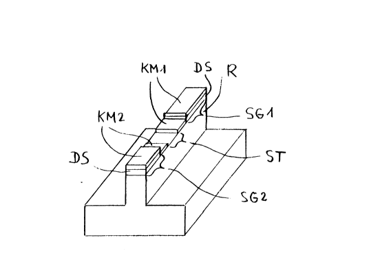
Fig. 5 shows the semiconductor chip with metal
contacts KMl, KM2 which are electrically separated
from each other. The separated contacts divide the
ridge waveguide R into two individually controllable
segments SG1, SG2. The segment transition area no
longer contains a metallization. This was achieved in
two steps. First, the entire chip except the segment
transition area was covered with photoresist in the
same way as described in connection with Fig. 3 for
the area of the contact metallization. Then, the top
layer still present in the segment transition area was
etched away by a wet chemical process, the
metallization in the segment transition area being
removed by undercutting.

Dessin représentatif
Une figure unique qui représente un dessin illustrant l'invention.
États administratifs

Pour une meilleure compréhension de l'état de la demande ou brevet qui figure sur cette page, la rubrique Mise en garde , et les descriptions de Brevet , États administratifs , Taxes périodiques et Historique des paiements devraient être consultées.

États administratifs

Titre Date
Date de délivrance prévu Non disponible
(22) Dépôt 1996-01-26
(41) Mise à la disponibilité du public 1996-07-29
Demande morte 2004-01-26

Historique d'abandonnement

Date d'abandonnement Raison Reinstatement Date
2003-01-27 Absence de requête d'examen
2003-01-27 Taxe périodique sur la demande impayée

Historique des paiements

Type de taxes Anniversaire Échéance Montant payé Date payée
Le dépôt d'une demande de brevet 0,00 $ 1996-01-26
Enregistrement de documents 0,00 $ 1996-04-18
Taxe de maintien en état - Demande - nouvelle loi 2 1998-01-26 100,00 $ 1997-12-19
Taxe de maintien en état - Demande - nouvelle loi 3 1999-01-26 100,00 $ 1998-12-17
Taxe de maintien en état - Demande - nouvelle loi 4 2000-01-26 100,00 $ 1999-12-16
Taxe de maintien en état - Demande - nouvelle loi 5 2001-01-26 150,00 $ 2000-12-14
Taxe de maintien en état - Demande - nouvelle loi 6 2002-01-28 150,00 $ 2001-12-17
Titulaires au dossier

Les titulaires actuels et antérieures au dossier sont affichés en ordre alphabétique.

Titulaires actuels au dossier
ALCATEL N.V.
Titulaires antérieures au dossier
KUHN, EDGAR WOLFRAM
Les propriétaires antérieurs qui ne figurent pas dans la liste des « Propriétaires au dossier » apparaîtront dans d'autres documents au dossier.
Documents

Pour visionner les fichiers sélectionnés, entrer le code reCAPTCHA :


Pour visualiser une image, cliquer sur un lien dans la colonne description du document. Pour télécharger l'image (les images), cliquer l'une ou plusieurs cases à cocher dans la première colonne et ensuite cliquer sur le bouton "Télécharger sélection en format PDF (archive Zip)" ou le bouton "Télécharger sélection (en un fichier PDF fusionné)".

Liste des documents de brevet publiés et non publiés sur la BDBC .

Si vous avez des difficultés à accéder au contenu, veuillez communiquer avec le Centre de services à la clientèle au 1-866-997-1936, ou envoyer un courriel au Centre de service à la clientèle de l'OPIC.


Description du
Document 
Date
(yyyy-mm-dd) 
Nombre de pages   Taille de l'image (Ko) 
Dessins représentatifs 1998-06-09 1 7
Page couverture 1996-05-23 1 17
Abrégé 1996-05-23 1 19
Description 1996-05-23 4 129
Revendications 1996-05-23 2 55
Dessins 1996-05-23 2 30