Note : Les descriptions sont présentées dans la langue officielle dans laquelle elles ont été soumises.
2 1~ 0
VOICE BUS FOR A COMPUTER BACKPLANE
Backaround to the Invention
Improvements in speech recognition and speech
generation technologies have made fully automated telephone
services practical. The combined requirements of computing
power and voice channel handling has heretofore been
accomplished with separate systems using interfaces for
communication. There is thus a need for a system capable of
providing both the computational power needed by the speech
technologies and flexible voice channel connections.
Summar~ of the Invention
In accordance with an embodiment of the present
invention there is provided a voice bus for a computer
backplane, the computer backplane having, disposed upon a
first face, pluralities of first and second connectors
distributed along the backplane, each second connector
substantially aligned with a respective first connector to
define a respective slot across the backplane, the voice bus
comprising: a plurality of third connectors disposed upon
the first face of the backplane and distributed along the
backplane, each third connector substantially aligned with
respective first and second connectors in a respective slot;
a clock signal line disposed along the backplane adjacent
the plurality of third connectors and connected to
respective pins therein; and a plurality of voice signal
lines connecting each of the third connectors to a
particular second connector.
An advantage of the present invention is the provision
of a voice bus in a manner which is both physically and
electrically compatible with the IEEE standard 1014-1987
known as the VMEbus specification.
srief Descri~tion of the Drawinas
The present invention will be further understood from
the following description with reference to the accompanying
drawings in which:
2124770
Fig. 1 illustrates, in a front elevation, a backplane
arrangement including a voice bus in accordance with an
embodiment of the present invention;
Fig. 2 illustrates, in a block diagram, the voice bus
in accordance with an embodiment of the present invention;
Fig. 3 illustrates a timing diagram for signals
typically carried on the voice bus of Fig. 2;
Fig. 4 schematically illustrates the voice bus of Fig.
2; and
Fig. 5 schematically illustrates the TSI clock
distribution for the voice bus of Fig. 2.
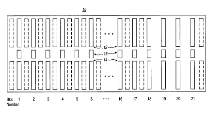
Referring to Fig. 1, there is illustrated in a front
elevation a backplane arrangement for providing a voice bus
in accordance with an embodiment of the present invention.
The backplane 10 includes a plurality of first connectors 12
mounted in equidistant spaced relation on a first surface
thereof. The backplane 10 also includes a plurality of
second connectors 14, each vertically aligned with each
respective one of the first connectors. The pluralities of
connectors first and second 12 and 14 together provide
connections to two respective transverse busses that conform
to an IEEE standard 1014-1987 known as the VMEbus
Specification.
A plurality of third connectors 16 are also mounted on
the first surface of backplane 10. Each of the third
connector 16 is positioned between and aligned with
respective ones of the first and second connectors 12 and
14. The plurality of third connectors 16 provide access to
the voice bus. Each horizontal position as defined by the
vertically aligned first, second and third connectors is
referred to as a slot. In the present embodiment, the slots
are numbered, from left to right, from 1 to 21.
Referring to Fig. 2, there is illustrated in a block
diagram, the voice bus in accordance with an embodiment of
the present invention. The voice bus is in the form of a
star. In the present embodiment, the slots connected via
the voice bus are slots 5 through 20, and the slots to which
21~7~
the voice bus connections are made is slot 21. Voice cards
20a-p connected to slots 5 through 20, respectively,
communicate with a time-slot-interchange (TSI) card 22
connected to slot 21 via the voice bus lines 22.
Referring to Fig. 3, there is illustrated a timing
diagram for signals typically carried on the voice bus. A
clock signal TSICLK is shown as a) in non-differential form
for simplicity. In the present embodiment, the clock signal
is a 5.12 MHz square-wave having a 50% duty cycle. The
synchronization signal (SYNC) is shown as b) and comprises a
single pulse having a width of one clock period. In the
present embodiment, the synchronization signal is a pulse
with a frequency of lkHz. A receive signal (TSI-RX) is
shown as c) in Fig. 3. The receive signal (TSI-RX) is a
serial 32-channel signal with 10 bits per channel organized
in frames of 125 ~s. The beginning of each frame (channel
0) is marked by the center of the synchronization pulse
(SYNC). The first eight bits are used for PCM bits, with
bits 9 and 10 available for signalling bits S and V
respectively. A transmit signal (TSI-TX) is shown as d) in
Fig. 3. The transmit signal (TSI-TX) is a serial 32-channel
signal with 10 bits per channel organized in frames of 125
~s .
Referring to Fig. 4, there is schematically illustrated
the voice bus in accordance with an embodiment of the
present invention. The voice bus provides bidirectional
point-to-point communications between a number of the
plurality of third connectors 16 and a particular one 18 of
the plurality of second connectors 14. For simplicity, only
the plurality of third connectors 16 are shown and the
particular second connector 18 between which the voice bus
extends. A subset of the plurality of third connectors 16
are connected point-to-point to the particular second
connector 18 via a plurality of lines 24. Each of the
plurality of lines 24 includes three (3) tracks for carrying
respective transmit, receive and synchronization signals.
In the present embodiment of Fig. 3, third connectors for
21~77~
slot 5 through slot 20 are so connected. The three signals
from a given slot are also connected to the previous slot,
for slot 6 through slot 20. Sense lines 26 are provided for
carrying a sense signal from a given slot to the adjacent
slots, to indicate the presence of a voice card in the given
slot that may use the serial link. The voice bus uses the
third connector 16 located between the two VME connectors 12
and 14 to carry the voice bus signals between the TSI and
the other VME slots. A clock line 28 including two parallel
tracks and a termination carries the differential clock
signal from slot 21 to slots 5 through 20.
Table A gives the pin-out for the third connectors 16.
The receive and transmit directions for the data are defined
from the view of the TSI (i.e. the TSI~s receive and
transmit data).
Pin Number Row A Row B
GND SxxCOUT *
6 TSICLK+ ** TSICLK- **
7 GND SxxCIN *
8 Sxx TX * Sxx SYNC *
9 Sxx RX * Syy SYNC *
Syy TX * Syy RX *
* -Slots 5-20 only
xx = Slot number (5-20)
yy = Slot number -1 (i.e. xx-l)(NC in Slot 5)
** -Slots 5-21 only
TABLE A
2124770
For Row A, the signals are: on pin 5 ground (GND); on
pin 6, positive portion of differential clock signal
(TSICLK+); on pin 7, ground (GND); on pin 8, transmitted
signal to slot number xx (Sxx_TX); on pin 9, received signal
from slot number xx; and on pin 10, transmitted signal to
next lower slot number to slot number xx
(Syy_TX, where yy = xx -1).
For Row B, the signals are: on pin 5, sense signal
output for a given slot number to the next higher number
(SxxCout); on pin 6, negative portion of differential clock
signal (TSICLK- ); on pin 7, sense signal input to a given
slot number from the next lower slot number (SxxCIN);
synchronization signal to slot number xx (Sxx_SYCH);
synchronization signal to next lower slot number yy
(Syy_SYNC); and, on pin 10, received signal from next lower
slot number yy (Syy_RX).
Table A shows how each slot has access to two 32
channel serial links, one shared with the next lower slot,
and the second shared with the next higher slot. The
sharing is based on exclusive use, where only one of the two
cards may use each shared link. This allows each card to
have 32 channels or for cards to use 64 channels when
adjacent slots not using any. To ensure that two cards do
not use the same link, two pins, Row B - pins 5 and 7, on
the voice bus connector are used as sense lines. The SxCOUT
pin (pin 5) must be tied to ground on all circuit packs
(voice cards) that connect to the voice bus. The SxCOUT pin
is routed to the S(x+l)CIN pin (where x is the slot number).
A card that uses two 32 channel serial links will have a
pull-up on its SxCIN pin. Such a card must check this input
to see if it is pulled down, indicating that there is a
voice processing card in the preceding slot. If this is the
case, then this card must not use the secondary 32 channel
serial link.
Referring to Fig. 5, there is schematically illustrated
the TSI clock distribution for the voice bus of Fig. 3. The
TSI clock signal is carried along the length of backplane 30
212~770
by two substantially parallel lines disposed adjacent third
connectors 16 (not shown in Fig. 5). The clock lines 32 and
34 are terminated on the backplane 30 with a 120 ohm
resistor 36 therebetween. The TSI card 22 includes a 10.24
MHz VXCO 38, a divide-by-two circuit 40, a differential
driver 42. The TSI card 22 drives the differential clock
signal TSICLK onto clock lines 32 and 34 via its third
connector 16 (pin 6, Rows A and B). Each voice card, 20a
through 20p, receives the differential clock signal (TSICLK)
via its repsctive third connector 16 (pin 6, Rows A and B).
The TSI card 22 also includes a differential receiver 44 and
a time slot interchange (TSI) switch 46. Each of the voice
cards 20a-20p includes a differential receiver 50.
Also shown in Fig. 5 is a standard VME card 52 in the
slot of voice card 200.
This is possible because the presence of the voice bus
does not interfere with the use of slots for standard VMEbus
compatible cards. The backplane providing the voice bus
remains completely compatible, both physically and
electrically, with the IEEE Standard 1014-1987, VMEbus
Specification.
In operation, the TSI switch allows connection of any
one of the 32 channels received from one voice card, e.g.
voice card 20b, to be connected to any one of the 32
channels transmitted to another voice card, e.g. voice card
20n. A TSI switch of this type is disclosed in U.S. Patent
No. 4,873,682, entitled ~Digital Key Telephone System~, by
George F. Irwin, et al., issued October 10, 1989, the entire
diclosure of which is hereby incorporated by reference.
The receive and transmit directions for the data are
defined from the view of the TSI (i.e. the TSI~s receive and
transmit data). The pin-out of the TSI card is shown in
Table B. The TSI uses the third connector to drive the
clock signals.
21~7~0
Pin Number Row A Row B Row C
1. TSICLK+ +5 VDC
2. TSICLK- GND
3. GND Reserved
4.
5.
6. S20 TX S20 SYNC
7. Sl9 SYNC S20 RX
8. Sl9 RX Sl9 TX
9. S18 TX S18 SYNC
10. S17 SYNC S18 RX
11. S17 RX S17 TX
12. +5 VDC GND GND
13. S16 TX +5 VDC S16 SYNC
14. S15 SYNC S16-RX
15. S15 RX S15 TX
16. S14 TX S14 SYNC
17. S13 SYNC S14 RX
18. S13 RX S13 TX
19. - GND +5 VDC
20. S12 TX S12 SYNC
21. Sll SYNC S12 RX
22. Sll RX Sll TX
23. S10 TX S10 SYNC
24. S9 SYNC S10 RX
25. S9 RX S9 TX
26. +5 VDC GND
27. S8 TX S8 RX
28. S7 SYNC S8 RX
29. S7 RX S7 TX
30. S6 TX S6 SYNC
31. S5 SYNC GND S6 RX
32. S5 RX +5 VDC S6 TX
Table B: TSI P2 pin designations (Slot 21)
212~770
From the point of view of driving the clock bus, it is
advantageous to drive the bus from one end, since to drive
from the center would reduce the impedance presented to the
driver by a factor of two, or would necessitate the use of
two clock buses with two clock drivers. Thus, in the
present embodiment, the TSI card is located in slot 21, and
slots 5 to 20 are each provided with one serial
bidirectional 32 channel connection to the TSI card.
For the present embodiment, the TSI_RX, TSI_TX and sync
lines are TTL level, point to point connections. The basic
track impedance specified for the backplane is as close to
100 ohms as possible, and to simplify the design of the
backplane the tracks for the voice bus should also have a
nominal impedance of 100 ohms. The driver should be an ALS
active pull-up bus driver, such as a 74ALS244. Since the
total track lengths will be longer than the maximum
recommended for unterminated lines, these lines should be
terminated at the receiver (on the cards, not the
backplane). The termination also ensures that the line is
pulled up when no driver is connected to the line, resulting
in an idle code of FF hex. This termination consists of
lK32 ohms to +5 volts and lK78 ohms to ground. The receiver
can be an ALS- gate.
For the differential clock lines (TSICLK +/-) RS485
drivers and receivers are used. RS485 drivers and receiver
were chosen since RS485 drivers can drive 32 devices, while
RS422 drivers can only drive ten. AS these are fairly slow
devices, the relatively short backplane appears as a lumped,
mainly capacitive and resistive, load.
To accommodate these relatively slow clock drivers and
receivers, the time slot interchange switch 44 gets its
timing by recovering a clock signal from the backplane bus
rather than from the input to the clock drivers. This has
the advantage that as the clock lines are loaded up by
plugging in more cards, the timing automatically
accommodates for this; also the differential driver delays
can safely be ignored. The receivers may for example be
~ 2124770
g
DS96F175 by National Semiconductor chosen because of
relatively high speed. Transceivers may not be used on
voice cards 20 because the associated drivers present a
substantially higher capacitive load than a receiver-only
5 device. To further limit the capacitive load on each card,
the clock stub tracks on each card should be less than two
inches long. The driver chosen for the TSI card may for
example be a DS75176B transceiver by National Semiconductor,
chosen because its timing is specified into a lOOpF
capacitive load, and because it is available in a small
package (eight pin). Since RS422/485 drivers usually drive
into a transmission line that appears as a resistive load
their timing is usually specified into 15pF.
It is also necessary to derive the sync pulses from a
15 source which provides them. Staggered sync pulses can be
easily produced using an eight bit shift register that
clocks the master sync pulse through.
Numerous modifications, variations and adaptations may
be made to the particular embodiments of the invention
described above without departing from the scope of the
invention, which is defined in the claims.