Note : Les descriptions sont présentées dans la langue officielle dans laquelle elles ont été soumises.
' ~ ~W093/15552~ PCIr/US93/O~)U98
5~ODEM II'~CLUIDII'JG AN EQIUIALIZER
FOR AUIPLITUDE ~ c l l ~:H
tOin~ i~ion by P~ef~ro,~c~ o~ bll~r IU. S, Patent
The ~ppiican~ hereby inc~.~r~l~s by r~f~r0nce ~. S. Pa~nt
4,m,s40, Michael D. Tumer et al., HFreqllency A ~ 3 ~hase J~er
Cancslar, issued Oct~ber 11, 1988, v~~llat~ nd with the sam~ effect as
thou~h th~ same patent were fully and ~mplete~ s~t forth her~in.
FisW of th~ In~r6nt;0.,
Thi~ application r~lates lo~ can,."unic~tion ~i~nal re~ivin~
appara~u~ induding, but not lim~ted to, ap~ar~us for comp~ns~iny the
r0ceiv~d communication ~i~n~ fsr ~ lea~t amplitude Jitt~r in order to
~0 ~ : : r~t~ modufated di~ital da~a ~
a~.~und of ghe In~ntion
rl~s~n;ly,:d~ c~ nwniG~ioll equipment (~DCE7, such as
modems, f~r ~xample, are ~in~ us~d ~o ~n~port ~ ta3 d;~ tween
2~ -~ dataa tenninal ~quipmer~ t~ SUCh as pe~onal compu~rs,
wo~ f ions-~an~ the lik~,:over challnels such as, -gor in~AoB~ telepllone
I ines~ ln s~me~ inst~ th~ commllnication si~nal is n~ula~ed to
inolude di~ital~ da~a in~ihe ~o~m o~ a train .of ~ym~ols based
>rh~te . -llin~d~ SIllit ~con~tellation ~ sig~al poir~gs. Ea~h signal point
30: -~ : otth~ ~r~ A~const~llation~ p~ sadi~ital~de orYalue. Each
symboli~modul~t~ slJ~, t=~ ial~atthesi~nalpoin~of~th~ S~
: ~ constell~tion ~ espo.~in~ to:the value desir~d to~be: r~ sented
r~6~inthe~ir~in~,a~thu ~nsp~ dov~rthe~h~ el. ~t~h~
:~: - r~ceiving D~E, the: ~.llbol~ ar~ e~lr..~ ~rom ths: c~ unication signal
:: :
: ~
~: :
W~ 93/15552 PC~/US93/0~
212x6~ ~ ~
and a siynal point is id~nti~ied fr~m a ~ a ¢onstellation of signal
points c~rl~rl~ondin~ to each ex~-~c.~ symbol. The si~nal points ar~
us~d to r~t~;~v~ the digital dE~a from the modu~ted communication
si~nal.
In c~mmunicatin~ the communication ~i~nals over ~he telephone
netw~ a source of disl~ hereof is known as jittsr "ict~.ti~" and is
caused primarily by the oouplin~ of sinusoidal dist~. tiGn from 60 Hz
power lines and/or the 20 Hz ~in~itî~ si~nal. An ~u~' ~er function is
comn~only used in the r~oeivin~ DCE to remove linear distortion from the
received communica~ion si~nals, but bQ~use of low up~ t~ ga~ns, an
e~llJali~sr i~ unable to r0mo~0 the jitter distortion c~ onents.
Jitter distortion is ~.--~,.is6J of phase and amplitude cG.~Ipon~nls.
it has beerl re~~ J tha~ ~he phase jitter c~ t ot the ~itter
~i~t~.tion has the maJor effact on modem pe,f~ ~ when usir:~
convolitiGnal receive consteli~tions fo~ standar~ data ~nr.~unication
at~in~ between ~ s. Accordingl3r, oontemporary modem
r~ rs include one or m~re pha~e jiffer ~nce~in~ circuit~ ~or reducin3
the ~inusoidal componeni~ ~f phase ~itter in the communication~
channel. An example o~ such a phase jmer cancelin~ circui~ may be
tound in the ~lichael D. Tumer et al. :U. S. P~tent 4,m,640, which pat~nt
has been ino4.~r~t~J by ref~ren¢e her~in~oJ~.
Re~ll~e ~f the ~r~ in si~nal pQiflt~; of the co~ ;nional reoeive
a~n5~ ;0.l5, ~he amplitu~ ter ~~ onent of the ji~ter ~ n has
littb' eff~cE on the modem's perfonn~nce. However, hi~her data b~ rate
osrnmunication i~ sontempl~ed ill th~ near futlJr~. Sin~ the bandwidth
he ~~ unication~channel~is substantial~ fixed, ;.~cr~asir~ data bit
ra~e~ is ac~n~plish~d by increasi~ ~he number of si~nal points of a
~ t ~3iVll ~nstsllation, ll,~r~y ~o.n~ sin~ ths distan~s ther~betwe0n.
- Consequent~r, hi~h speed ."~e.l.s inoorporatin~ th~e co,~pr~sse~
r~3i~ ~4n~t~11ations are lik0iy to b~ mor~ s~pt;l~le ~o amplih~ jitter.
' ~ For example, in a contempl~ted 19.2 K b~s per ~ hi~h speQd
Ill~Chl r~ivar a~ t~le 8~ 2~6 amplitude ptter can ~ffect the rn~."'s
p~ ,al~. Under:these ~.~ition~, amplitude ~itter ~f~ the ~i~nal
to .3isl~ n ~; ~i,.,ance o~ the hi~h ~peed modem in the same way that
( ~wo 93/15552 2 1 2 ~ ~ O 9 PCr/US93/OO~g8
phase jitter ~f(0~t~ ~. fo~ n~e of a lower speed ~ . Ao~orJ;n~ly, it
is desirable f~r the cortamplated hi~her speed modems to include not
only phase jffler cancellation to compliment the ~ er function
~heraof, but al~o to include an amplitude jitter cano011in~ Sun~ion to
fusther i~ .rov~ ~c.fu~ nce.
SlAmrn~"~ of the Invernion
A .n~J0n~ is ~ d for receiving a si~nal, the si~nal includin~
modulated symbols based on a predet~rl,lin0J con~tellation ~ points,
each point repros~ a symbol. The I~ l inclu~
me~ns for ekl~d~Ain~ mod~ t~ sym~ls to provide an e~i~d
symbol, R(k), the e3~t~t~ symbol includin~ amplnude jigter disl~;o."
iJ6~ iny means hr identifyin~ a ~nal point Pn(k) of the
pr~detennined conslellation c~ o~din~ to ~he extrac~ed 5~.-~l,
based ~n a pr~de~errnined cnteria;
d~termining: means ~or d~ter,l,inin~ an error ~i~nal represe,~t~ti~,o
ot the amplitude jitter ~ tiG.) based on the extrac~ y..~L~I an~ the
si~nal ~in~; and
compen~satin~ means ~05~0n~V~ to ~he erro~ si~nal ~or
2~ oo~.l~nsatin~ least one slu~ ent e~ syml~ol for the
amplitude Jitter~i~.bon prior to the :idenfflyin~ means identifyin~ the
signal point ~..es~ndin~ th~to.
- Brief ~e~;~,l;on of the D~awin~s
FIG.: 1 is a~block dia~ram schematic o~ a flrst embodimer~t of a
modem includin~an ~egualker for amplitude jitter, in ac~rdan~ wi~h the
FIG~ 2 i~ a ~raph depictin~ a ~i0nal point const011a~ion.
FIG. 3 is:a bl~ schematic o~ a fir~t ampl~ude j~ter
FIG. 4 is a bl~k ~i ~.O ,. s~ atic dspictir~ furth~r de~ail for the
amplitude j tter ~.~r~of Flt~. 3. ~
~ FIG. 5 is a~block ~ dll~ schcniatic de,~ctin~ a 3~co.,J amp~itude
jiner tra~ker.
WO ~3/15552 ~ PC~/US93/o~38
- 4 -
,
~)et~led C~ ;plio-,
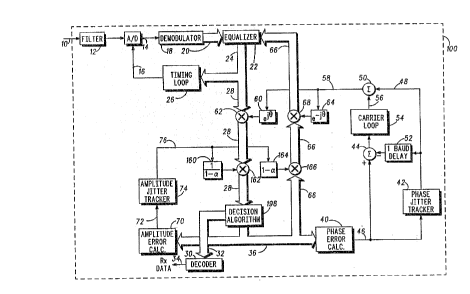
FIG. 1 is a block Jia~r~". sehematic of a r~n, 100 includin~ a
~iv~r th~t is bein~ used, by way o~ example, as a receivin~ ion of a
6 WE. Referrin~ to FIG.~1, the rscaived ~i~nal 10 tha~ has been
t~n3,~0rted by a ~ nn~l which, for oxample, may be a tO13~ 0nl3 line,
incl~rl0s jffler ~istonion. Genera~ly the si~nal 10 will include rn~u!~ted
symbols based on a pr~eterrnined constellation. As is known, the
constellati~n inG~ es a piurali~y of points, each point repr~sonli.~ a
symbol. Each symbol, in tum, repr~ssnts a value to be l~ s~orted.
The i.~."i.~ si~nal 10 is ~i-st filtered and amplffled by a
conventiQnal .ow pass fi~r 12 whieh rnay include an automatic ~ain
co~ el cir~uit. Next, the fiHered si~nal under~oes analo~-to~i~ital
("A/E)7 c~nv~r3iol~ by a converter 14 at a contn~ mplin~ rate
1~ ~ovsm~cl by a samplin~ signal 16. The~ di~al da~a of the AJD
~ ter t4 is ~nlc~ '~ by a oonventi~na~ demodulator 1~ and the
dernQ~ d output 20 is et~ ~ by an equalizer function 22. In the
p7esent emb~iment, the equalizer may be of the IL~S~ bast means-
squar~ , for example.
~ The O~ltpUt of the e~lu;ll ~er 22 :is an equalked r~aive si~nal 24
which ~overns a conv~r~tiorlal 1imin~ bop 26 to pr~vide the sampling
si~nal ~6. In th~ present ~n~ n~, the samplin~ rate is a~justed to
a,~p~xin~te~ four t3mes th~ s~.nl,ol or balld rate of the Incoming train of
s3~-"~1s ~orrning:the r~ived si~nal 10. The oo,~ o~ ol~ ls
14, 18, 22 and ~6 provid~ ghe function of ex~,~in~ ~he modula~
v ~: sy~ ot~the ~rain from~th~ r~eiY~ nal 10 and p~.dt.,~ them, as
exl-~v~3 sy~ ls, to a ~e~io~ aborithm 198 via ~ha si~nal tine ~8. In
~o~rdl, the kth e~l~d ~ sym~l may ~ ~e~er~ to as P~(k~.
In the ~J~ ~ si~n al~or~hm 198, a signal poi~ Pr,(k~ ot the
pr~dete~ J&J~ r~ceive conste~lation ~.-~sp~ndin~ ~to an ex~.~cl~l
ymbo1 R(k)~is~ idenWi~ bas~d on a predetermined ~ ~ia. In th~
pr6~3~t 13.~ .6nt, the c~eria used ~or si~nal poing id~n~tfk ~l;on is
bas~d Oll the rlosest si~nal point o~ th~ ~eceive constellatiofl ~o the
WO 93/15552 21 2 8 6 0 9 PCII/US93/00098
e~ll~ted symbol. Onc0 ths si~nal point Pn(k) is iden~ified9 ~ may ~e
used to r~t~ the vaOue ~r,~spo"-J;. s~ lhereto.
FIG. 2 is ~ ~raph which iIIus~ es the si~nal point idsntifi~ation
~)r( ~e~s. Since each e~ ~l symboI inc4Jdos an i~pl,dse 1 aQd
quadra~ure Q ~n~ ent, the al~ ~ (or~ axis and or~ le (or ~r)
axis of the ~raph ra~l~s~nt the respective I and Q ~."~nents. While th~
graph ~ FOG~ 2 exl.;t;ils on~ quadrant 1 ~f the ~c~ ~ns~ on
includin~ si~nal poin~s P1-P4, it is unders~ood that the p.inciples
~esc~i~d also ~ply to the other thr~e quadrants of the r~Qive
con~t~ on as well.
Accor~ Iy, an e~l,a~6J sym~I may be r~pr~sG.,t~ by a ve~or
~uch as that shown by vector P~ and each si~nal point m~y be
~tple~~SII by v~ors as w~ll. In the pr~sern e~ , arr~r wctor~
E may be measu~ ~rom each of the $i~r~1 points of the ~3iv~J
consl01lation to the t~At~t6J symboI ve~or ~ under consider~tion and
~he si~nal point havin~ the smallest magnitude error vector is con~ide~d
the identiff~d si~nal point. In FlG. 2, si~nal poir7t P1 has the smallest
error vector to the e)~ ;J symbol vecto~ P~ and thus is con~ ~l the
c1~5~
Qnce ~he d~sion:a!~orithm 198 identifies the si~nal point Pn(k)
c~ s~n~ih~ ~o the e~t~l~l s~ l R(k), ~he si~nal point Pl,~k~ is
appliQd to a ~ ~r 30 t~v0r ~i~nal path 32. Ins the d~oder 3~, the
di~al data oor,- 5~ to the idefltifi~ si~nal pdnt Pn(k) iS I~liB~d~
The da~a is then output o~ path 34 as reo~iY~d bltS.
In addition, the decision al~ori~hm 198 applies the ~-s~n~J
- error si~nal E(k), that is based on the ~ ~ symbol R(k) and the
si~nal poin~ Pn(~, to th0 ~ualizer 22 over si~nal pa~ll5 3B ~d 66. The
e~u~ r 2~ Incl~dqs oompen~lin~ rnaans r0sponsiv~ t~ ~he error
si~nal ~or ~ an~a~in~the ~v~s~ e~ e~ l symbol, R(k~1). Since
~h~ e~ er 22 is ~ t~ ~efor~ the dec ~ion a~ 8 in the
~i~nal path, th~ x~ s~lle~t comp0ns~ion will ~ur pnor to ~he ~d~ion
ai~ri~l~.,l identi~yin~ the si~nai pOillt Pn~k~1~ coll~~ o tha
F~ ~seqllent e~ .1 s~ 601. Thus, the e~ltJali7er 22 u~ilizes the er~or
~ignal E(k~ ~or adju~t~ th0r~0f in or~erto reduc0 the n.~.~ de ~f the
WO 93/15~;52 PC~IJS93/0
b60 9 - B -
subsequenterrorforthe~IJ~s~ ente~ lsymbol,R(k~1). As
l above, the equalker 22 i~ ~enerally unabl0 to remo~e jitter
disl~.lio,. tr~m the r~i~re,J, signal.
For purposes of expl~nation, the ex~s~ .J symbol R, as ~epicted
in th9 ~raph of FIG. 2,'iS considered to incllJde only Jmer ~ t~rtion.
Aocor~lin~ly, the error ~ or E ~hen is oalH~ ~ o~ both an amplnude
jittsr distortion cc r"ponent anct a phase jffler distortion c~ onent. In the
~raph, the amplitude ~itter ~ ,1;on cG."ponent is ~o~ a~nted by Fa and
is in line with the vector of the identified si~nal ~ir~ P1~ ~n a~i~ion, the
1 û phase ~iner dis~Drtion component is r0pr~sented by Ep and is
perpendicular to the idsntifled si~nal point ve~or.
To co~."~ns~ts for the phase jffler distortion co,-"~o"ant, the error
si~nal E(k) of path 3~ is applied to a phase enor calculator 40 which
separates out a phase jffler distonion distor~ion error si~nal 46 lll~r~i.u",
that is appli~d to a ph~E3 jittsr~raclcer 42 an~ also to a summ~r 44. The
phase jlt~er i-ac~r 42 is ~es~sonsive to the phase. jiner dist~rtion error
~i~na~ 46 to provide a phase ~itter ~;.,t~ an~e si~nal 48 that is
app~ied to a summer 50 and ~so to a delay gun~ion 52 which delays th8
phase ~i~er ~ iol~ an~le term app~a~ ately î baud or ~,-~ol time
interval b~ore SulJt~ it from ~h6 pha~ jitter disltortion term 46 in the
summer ~4.' .The outp:ut of th~ summe~ overns a ~mer loop function
54 to provide a carrier an~le ~nn 56 t~at is ssumm0d with the phase jffler
ti~ angle teml 48 in ~he summer 50 to produ~ a t~tal phase angle
~n~p~n~tion term 58 that is .~"~r~nt~d by ~ bol q.
'- A phase :compensatin~ ~nal ~ is ~om~d 1r~m the oompensatin~
signal 5~ in th~ block 60 and ~sed ~o ~mp~nsa~ ub~e~uent
à~tt~ ymbol P~(k~ t path 28 utilizin~ a mu~ipOier 62 ~ po5v~l in
the si~nal path 28. In ~J~I lion, another ~ompensa~ si~nal e~i~ is
9Gn~ in a block 64 fr~m the compen~tL~ si~nal 58 and is used ~o
3û ~n~ the error si~nal of path 36 to effe~ a phas~
err~r si~nal 6fi ~or adjus~ing the ~ 7er 22. In the p~
emb~limen~, ~he c~.."~ns~ling~ si~nal of block &4 mu~iplies the ~rror
signal usin~ a ,.~lttplier ~8 di~r~ in the er~r si~nal pa~h 36. For
mor~ detai!s of tha ~o~e~;ny ~5~1 il~ phase jitter ~ . ti~n
WO 93/15552 2 1 2 8 S o g Pcr/usg3/ooog8
~7 ~
,~nsation por~ion of the modem, refer to the afo.~m~r.~ioned U. S.
ralenl 4,77?,640 which has been ~nco"~r~d by reference
hereinabov~.
Further in re~ard to the ~r~sc.~t embodiment, the error signal E~k3
o~ path 36 is applied to an amplitude er~or calculator 70 for denvin~ a
nol-"ali~J amplitude jitter di~tor~ion error si~nal 72. In the "r~nl
~nl~otli.~ , the c~la~tor 70 projects the error vector E(k) of the
cor,l.3~0nJ,n~ ex~ d si~nal P~(k) onto the vector of the Tdd.~tireJ
signal point ~n(k) to derive an u,~Gn"alized error signal Ea(k). In
~ ", th~ ~rror signal Ea(k) is no~ aliL~ ~y ~ it by th~ absolu~e
vallJe of the identifi~ si~na~ po3nt vector Pn~k) ~o derive the nG~ alk~d
error si~nal En(k) 72.
In the present e3~ en~, the unr,~ ali~J error si~nal ~a(k) is
d~rived in the ~ tor 70 based on the folio~.~;ny equation:
Ea(k)= EXPX ~ EyPy 1/2(ExPy-EyPx)
,_~
wher~: ~
~X a the inpha~ ~O~ n~ E(k),
Ey - the ~l~Jqrl~ur0 ~.I"~)erlt of E(k~;
PX - the: ;npha~e ~.,~onent of Pn(k); and,
Py = th~ quadratur~ co"-ponent ~ Pn~k).
~ ~ M~rQ~Yer, ~he nor-,~aIi~ error si~nal E~(k) is dl~rVed based on
the ~oIIowin~ ~J~ffon:
: E~(k~
Erl~k) =~ ~ lPn(k)l ~
: , ~
In conn~iorl with th~ compensation of th~ ampIi~ude Jitter
30 ~b~ n, an~ampI~tude jittert~k~r 7~ is r3sponsive to th~ norm~ize~
err~r signaI En(l~) 72 to pr~ e a ooIIIpO~ tiIl~ si~naI over path 76
FIG. 3 is a bIock Jt~y.dn. scl.~...~,c of an ampIitude ji~t~r l,~cl~r
74 suitable ~or use: i~ th~ &.~ nl ~ FIG. 1. Sillce th~ ampIitude jitter
WO 9~ 552 P~/US93/0~
6~ - 8-
dist~.rtiG,~ in~ dQs at least one sinusoidal ~r."~n~nt havin~ an
amplitude and a frequency, the amplitude jitter tracker 74 inclu~e~ a
second~rder ph~se locked bop 94 and a phase accumulator 98
responsive to the nur..-alked error signal En(k) for pl~Jitl~ a -
compensating signal frequenc3~ value 8A and a ar~u~ 82 r~spon:,iv~ to
the error si~nal for pr.~ )$; a compensating si~nal amplitude value e1
at 86. The amplitude value 8~ and the frec uency value 84 are applied to
a muitiplier ~8, wh~ch pro~des the composite co,..~ns~ting si~nal 76,
represented by the Greek symbol a.
The functien of the amplitude jitter tracker 74 in the present
embodiment, is to match the compensating si~nal 76 to the arnplitude
jmer ~;_t~.tiGn of the extracted symbols such that compens~t;Gn thereof
conver~es the cG.-~ ~F~ndin~ error si~nals to a steady state value,
preterably substantial~ zero.
More epecifically! tor each e~t~ ol R(k), the nGrlllali~er
block 90 normalizes the cor-e~ din~ error si~nal En(k) 72 by ~i~iJing
with the derived amplitude term c1 to r .."uv~ ially amplitude
~/a~i~tiGns thereof. The ou~put of the no~-.~li~er 90 is then applied to one
input o~ a muWplier 92. ~ The olltput of the muttiplier ~ drives a seco.,~
order phase~ bck bop 94 that i8 used ~0 track and update an incremental
phase 96 of th~ frequen~ te~m;in the proper dir~ion. The resul~in~
incremental phase l~ si~nal 96 is applied to a phase accumulator
98 which g~nera~es~a phase term~f3 for the s~Jbs~ent extracted symbol
R(k+1 )~
~ : The phase term ~fj is dela~d by a~p~oxi.. ately ono ~y.,ll~ol time
i nt~rval by the~delay bloclc 100 and applied to bl~102 wherein the sign
ot cos fl is deriv~d~and~applied to another input of the rnu~tiplier 92 for
muttiplying the norrnalized erro~ si~nal En(k) 72 ~o insure that the phase
lock loop 94 is ~ 9 the inc~ ,ental phase 96 in the ,~,ro~r ~;.eclion
~ ~or each e~ symbol.~
In ~ tiG~), the compen~t;n~ signal ~r~quenc3~ value 84 is
;~ computed by establishing the sine of the phase tenn ~l in bbck 104. In
op~ration, the~conipensating si~nal irequency value 84 is ~ t~he~ to the
traquenc~ of the~ sinusoidal amp'itude jiner 6LslGrtio~ ot su'~se1~ lent
;~ 0 93/15S52 2 1 2 8 6 ~ 9 PC~/US93/000~8
exl~ J sy..ll,ols such that ~ .)~tion of the sul~ snt e~ .~eJ
sy~ ols w~th ~he ~requency value 84 conv0r~es ~he c~r~ 3~ error
siy"~ls to slJ~t~rltially zer~ values.
Mo~ver, the arcuit 82 of the ampl}tude jitter tracker 74 op~r~les
to corr~l~ts the normaUzed error si0nal En(k) 72 wlth the 1raquency value
84 via a O~ i delay thr7ugh block 10~, thus substantially
removin~ any sinusoidal va.i~lions from the ampli~ude value 86. The
circalit 8~ operates ~o match the amplitude valu~ 86 to the amplitude of
the simusoidal con"~,onant o~ ~he amplitude jit~r distortion such that
con)p~ tion of s~ e!llJ~nt e)~ e~ed symb~ls with the amplitude valu
~ COn1/e.S,~5 the co.l~,s~onJil)~ error si~nals to ~ n~;al~ zero
values.
FIG. 4 depicts the seco~ ord0r phase lock i~sp 94, phase
accumulator 98 and the dr~uit 82 in ~urther ~ail. Re~errir~ to FIG. 4, the
output of the mul~ipiier 92 is operated on by a ~ain term w;21~ in block
110. Further, the ~utpuf of bl~ 110 is a~umulat~d in an accumul~tor
lGrl~leJ by the ~ummer 112 and a one-symbol tim~ erval delay 114.
The ~cum~ ~esu1t is applied to one input of a summer 116. The
output o~ multiplier 92 i8 also operated on by a ~ain terrn awlT in btock
- 2a 11~, wh~r~ a is a ~onstant, and the resu~ is applied ~o another inpu~ of
th~ summer 116.: The resu~ of the summer 11 fi b~omes the ~sti-n~
incremental phase 96 forthe~s~bs0~uen~ e~ l,ol and is
applied to the a~cumulator 98 th~ is I~ by a summ~r 120 and a one-
sym~l delay 122.~ :The output of tha~a&cumulator 98 p.~ s the phase
te~ fl forthe~ls~s~1uent e3nI~t~ symbol.
Mc~o~-, the drcuit 82 ine~ c!9S an adaptiv~ updat~ filter. Mor~
particularly, th~ error signal En(k) 72 is mu~tipli~ by the fr~uency Yalu~
- ~ 84, dslayed by a one-s~ ~l tim~ interval 106~ in ~ multiplier 1~6~ The
~utrln of the muWplier 126 is operated on by a ~ain K in bl~k 128 and
: the resultant si~nals ~r each of th~ ct~l symbols ar~ accuml~e~
by an a~cumulat~r f~,r-"eJ by a summer 130 and a on~symbol time
- interval delay 132. ~: The accumulation re~ults in the amplitude v~ue 86
: ~ which is s~ nlially fr~ o~ sinusoidal varia~ions, and has an average
that is ~n~lated with the amp'~!d~ ot t~e en~r signal En(k) 72.
WO 93~15552 PCI'/USg3/~Q8
0 9 - 10 -
FIG. 5 depicts an a~emate ~..~li,.~nt SOO ot an amplitude ~itter
tracker 74' suitable for use in the mod~m of FIG. 1. This altemate
e~ .d includes a linear predictor tunction that is r~sponsiYs to the
noln-~li ~J error si~nal En(k) 7210 provicb the co..~ps.,sating signal a 75
~or use in co.--p~ris~in~ subs0f~ nt e~ l~eJ sy.-lbols. The error si~nai
En(k) ~ is ~mpe.~sat~J by a si~nal tonned as a function ot the
co.-,pensatin~ signal a 7~ in a multiplier 140 to provide an interrnedia~
error si~nal EA(k)~ In the present embodiment~ a block 142 forms the
signal for c~mp~ns~tilly the error sbnal as 1 -a. ~;till further, the
oo---pensatiny si~nal ~ 76 is SUI~tl ~t~J from the interrne~ te error signal
EA(k) in a summer 144 to pr~W~ a second intermediate error si~nal b(k).
A delay line 146 having a plurality m o~ tapped delay ~tages is cper~tive
to conduct the seai.,d inte""eJiate error si~nal b~k) throush ~he plurality
of delay sta~es thereof. The ~ntents of each sta~e i bein~ operated on
by a cor-_sp~ stage gain q to provWe a ~ &o.. Jin~ plurality of
tapped o,np~t si~nals~which are sumrned in a summ~r 148 to produce an
estimate 149 of 1he compensatin~ si~nal a 76 for th~ ~u~sequent
extr~ ol. Each of the sta~e ~ains q is ~ '~ as a functien of
. ~ : theintermediate;error:si~nalE~(k)~asshowninthebock150. Aone-
- ~ symbol de!ay~ 152 oper~tes:on the estimate 149 to derive ~he
.atin~ signal a 76.~
Re~ening~ a~ain~to FIG. 1, a si~nal is fomn~d as a ~unction of the
Co~ Q signal of path 76 in the~block 16010r use in cG~"pe,-~ling
the wbsequent e~ .,1~J :symbo1 over path 28 to provWe a compens~tsd
25 : eal,3~,ted syrnbol:;for use~in the decision al~or~thm 198 to identify ths
signal~ points~ ~nding !her~to.. :In ~the~ pr~sent e~ ent, the
e~ s~ ol ef~path 28 is~mper~ ed by the si~nal (111-a) fonned
- : - ' ~ by block 1~0 by mupip~in0 the eAl-~ed s.yl"~ol thereby utilkin~ a
n ~ muniplier 162~ ose~ in the path 28. Similar~y, the error signal ov~r
30 ~ path ~6 for~use in~adjusting the equalker:Z~is~ sated by a si~nal
a) ~..l.e~l in ~block 164 as a ~un~ion 0~:the;co~ nsatin~ si~nal a 76
to ~ W~ a:~ nsa~J error stgnal over~path 66. In the pr~sent
~"~ .ent9 the siynal f~.--,~ by block 164 muttiplies the error siQnal of
path 6B by a muttiplier 166 ~;~s~ in the path 66.
f ~wo 93/~5552 2 1 2 8 ~ O 9 Pcr/US93/00098
Mor~over, the eQ11-1 70d exgra~ted symbols of path 28 are
compo.~ J for both smpl~ude jitter distortion and phase jttter di~ lion
utili~in~ tha ~sp6~;~ly col~s,~ndi"~ ~mplitude pner tracksr 74 and
phase jit~er tracker 42 in connection ther~with prior to Wentifyîng the
signal points thereof through use of ~he ~ ;on aborithm 19~. Once the
e~ oleJ sy-nL,ols are compens~l~J ~orthe ~itter ~i_to.~ion, ~he r0suttant
compen~fl~d symbols ar~ closer to their ir~e.,J~ nal poir~s so that
identil;~tlon ~f ~he ~r~r si~nal point will be a~hisved, thereby
imprwin~ perforrnance of the ",oJ~m r~iY~r.
Retuming a~ain to FIG. 1, ~hose skilled in the art will ap,~,reciate
that the fitter 12, the A/D oonverter 14, the demodu~or 18, the timin~
ioop 26, the de~er 3~, and the decision a~ofithm 198 depicted therein
typiai modem funclions, whereas the remainin~ ~~n-~nls
ooll~&:tiJ~ly inter~t to p~ r"l a ~eneral ~ualizin~ functiosl.
1~
As explai~.eJ hereinaL~o~e, jitte~ Jis~ftion in~iud~s both a phase
~,.,~n~nl and an ampl~ude ~mponen~. A major sl~ cGfllin~ of prior
modem equalizers is th~t they have not ~l~ssed ~he problem o~
plit~ er distortion. At hl~her b~t ~es such as, for instanc~, 19.2
~ s per se~r ~ e amplitude jitt0r disto~tion is cnJaal to the
~ti~f~ y perF~r~ ~ of the mod~m. For example, an amount of
amplitude ji~r ~I;Otti~ n as low as 5% will CaUS~t rel~;;~ly hi~h leYels of
~ivod b~ error~l p~oL ~ly ~t least 3~h. Thus, ~he bi~ ~rror rate (~BERn) =
~.03. In modem communication applications, such ~ hi~h bit err~r ~ate is
nom~ u~laF~pt~le, and i~ would Iy mean ~h~t the modem
couW no~ b0:used in th0 ~e~i~ appli~ion.
The f)r~s~nl m~dc.., including an ~ er ~or amplitude ~itter, in
ac~ll~J~nce with ~he p~s~rd inv~ntion, combats this probbm, ~w~3bslr~
by ~ff~ctiv~ly compensati.)~ for at least nin~ty nin~ ~n~,~ (99~/O) of ths
unwanted arn~!itude jitter ~ lion. Stat~d other~nse, ~he am~unt of
unoompensated a~ itude jiffer di~,tion r~mainin~ in the e~ ~ed
:: sy,nbol~ is r~ by a ratio o~ ,at&3y ~00 to 1.
Moreov~r, such a modem, in ac~or~L.~3 w~th ~he ~ e~
in~ ;on, provid~s an even graat~r impr~Yernent in perfol-t)~nc~ when
WO g3/15552 PCI-/US93/O~B
60 - 12-
measur~d in terrns of b~ error rate, inasmuch as the co. ~ ~r.Jir,~ bi~
errors in the receiv~ data stream will be r6-luc~ by an even more
slu~ tial r~ti~an i""~ru~ement, in fad, ~f at ~east a ratio of 10,000 to 1.
Thus, the end user may be ex~ed to enjoy a bit error rate of -
S z~pio~ ately 0.0003%. Thus, the BER = O.OOOOQ3.
The over-all ~il~8tit to the user, ot course, is obtainin~ a modem
product that will work in a high-speed application. This is b~ se, as a
direct result of a modem in a~r~lance with the presenl inver~ion, the
amplitude jitter disto\tiGn and cc~ ~ndin~ bit rate are i,."~ s~ to a
degree that ~ m speeds of 19.2 KBits per second, and perhaps
5~r~r, may reliably ~ achieved, with saitisfactoly levels of re~iv~d b~
errors.
While various ~ ents of a modem in~udin~ an ~ er for
ampl~tude ~ffler, aco~ to the present invention, have been Jeso~
hereinabove, the scope of t~)e inwnfion is defned by the followin~
claims.
::
:
. .