Note : Les descriptions sont présentées dans la langue officielle dans laquelle elles ont été soumises.
wo ssnss32 . ~.,~,.. ,~.c :~ss
2188128
-- 1 --
IMPEI~ANCE T~Mr7T A'rOR
pTT~Tn OF T~T INVENTION
This invention relates generally to; - nre emulation
and more partieularly, to a low eapaeitanee i - '~n~e
emulator well ~;uited for aetive ennA~r1 ~r termination.
RAI .~1 'UNI~ OF T~7T INVTNTION
It is well known to terminate a ennAIlrtor with an
- '~nre whieh is ideally matehed to the dynamie i - nre
of the eonduetor in order to reduee signal refleetions and
eoneomitant degradation of data transmitted on the eonduetor.
One sueh terminator eomprises a resistor having a resistance
value - ;n5-lly matehed to that o~ the conductor. While the
nominal resistance value may match a typical ennAI~etnr
-'-nCe, tolerances ean affect the eonductor and resistor
- nrD~:, thereby degrading the re5ulting ; ~ nre
"match". IIJLe:O~L~ the resistance value of such a terminator
is f ixed so that its use to terminate conductors having
different dynamic; - is precluded.
Another type of terminator utilizes an active device and
thus, may be referred to as an active terminator. An example
of an active terminator is one utilizing a field effect
transistor (FET) biased to saturation. In this operating
condition, the FET has a highly non-linear, current source
characteristic which generally does not reduce signal
reflections as well as terminators having a linear,
~ubstantially re~istive chAraeteristic.
W095/29532 . . . ~ ,r~lE11
2188~2~ --
~ r~MMARY OF THE INvr~NTIoN
In accordance with the invention, a low capacitance
- n,e emulator is provided for emulating a selected
& having a substanti~lly linear characteristic. The
emulator i5 well suited for use in terminating one or more
conductors of a hi~ ,eed data bus where accurate, low
capacitance termination is critical. the low capacitance of
the emulator ensures that when the terminator is coupled to
the bus in a ~;~cv . G~ L mode, the emulator does not adversely
affect the conductor i -~nre. The i ~ n~e emulator
utilize6 an emulating FET operated in the linear region. The
linear operation of the emulating FET provides an ; - ~nre
acro6s the drain and source electrodes of the FET which is
sub6tantially resistive (i.e., characterized by a linear
rela~ i rmch i r between the current through the FET and the
voltage across the FET). This resistive characteristic is
particularly ef ~ective in signal termination to reduce
unwanted signal reflection6.
A control circuit i5 provided for maintaining the
emulating FET in the linear region of operation and includes
a control FET having like characteristics to the emulating
FET and coupled in series with a resistor. The control FET
is operated in a closed-loop fashion 80 that its conduction
is controlled to maintain a predet~rminD~ voltage thereacro66
and more particularly, to provide an i -'-n-e having a
pr~ t~rminF~d relation~hir with respect to the resistance of
the resistor. The emulating FET receives the same gate
signal as the control FET, thereby causing the emulating FET
to provide an; - nce proportional to the i ---nr~e of the
control FET. The resistor may be a trimmable or a variable
resistor 80 that the i ---nre provided by the control and
emulating FETs can be adjusted by trimming or adjusting the
value of the resistor accordingly.
In one F-~nhQ~ L, the emulating FET provides the
termination; - n~e of a signal transmission conductor.
More particularly, the emulating FET is coupled in series
WO95129S32 ,~ IE~,4
2l88~28
-- 3 --
between a voltage regulator and the conductor and the
resistance value of the resistor is selected or trimmed to
CVL~ UI~d to the dynamic; ~ nre of the conductor.
Use of the i -' ~ emulator in signal bus termination
is advantageous due to the linear, highly resistive
characteristic o$ the FET in the linear region of operation.
More particularly, this arr~ serves to reduce signal
ref lections on the conductor, thereby enhancing the
effectiveness of the terminator. IIc,~u~.~L, simple adju~i n t
of the termination i -~nre is achieved by trimming the
resistor of the control circuit to ensure that the emulating
FET provides an ;, -~-nre cur r .~ 7in~ to the dynamic
- nce of the bus.
BRIEF DE~ KTK~lON OF THE DRANINGS
The foregoing features of this invention, as well as the
invention itself, may be more fully understood from the
following det~iled description of the invention in which:
Fig. 1 is a schematic of an; ,---nre emulator in
accordance with the present invention;
Fig. 2 shows illustrative characteristic curves of an
NMOS FET;
Fig. 3 is a schematic of an active bus terminator
ut; 1 1i 7; n~ the ; ~ - ' ~ emulator of Fig. l; and
Fig. 4 is a detailed schematic of the active bus
terminator of Fig. 3.
DESCRIPIION OF THE ~K~ !;L) EMBODTMFNT
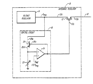
Referring to Fig. 1, an; -` nre emulator 10 is shown
to include an active emulating device 12 f or providing a
substantially linear pr~d~t~rm; n~ i , - ' nre. The active
device 12 is a metal oxide field effect transistor (NOSFET)
having a drain electrode 12a, a source electrode 12b, and a
gate electrode 12c but alternatively may be any suitable FET.
The predet~nin~tl i - _ is provided across the drain and
source electrodes 12a, b of the FET 12 which, in the
wossltss32 ~l/IJJ~J.'~l el1
~188128
-- 4 --
~ i - L5 de6cribed herein is an NMOS FET 12 . The
i _ - ' nre emulator 10 further inrl~ oc a voltage regulator 14
providing a regulated voltage V"~ and a control circuit 16
coupled to the gate electrode 12c for controlling the
operation of the emulating FET 12. More particularly, the
control circuit 16 maintains the FET 12 in its linear region
of operation in order to provide the prD~l~to~nin~A ir~e~lAnre
with a linear, resistive characteristic.
Referring also to Fig. 2, illustrative characteristic
curves of an NMOS FET, exemplary of the emulating FET 12, are
shown to include a linear region of operation labelled 28.
The linear region 28 is characterized by a linear
relation~hi~ between the current IDS between the drain and
source electrodes of the FET and the voltage VDS across such
electrodes. Operation of the emulating FET 12 in the linear
region causes the i - 'Anre across the drain and source
ele.~Lodes 12a,b to approximate that of a resistor. A
resistive ~ -nre i5 particularly advantageous where the
-` ~ emulator is utilized in terminating one or more
c~n~ rtors of a signal trAn~ ion bus, such as c~n~ tor 18
coupled to the source electrode 12b of the emulating FET 12,
in order to reduce unwanted signal reflections. The
characteristic curves reveal that the slope of the curves in
the linear region ( i . e ., representative of the drain to
source 1 -'Anre) varies in proportion to the gate to source
voltage VGS. In order for a FET to be in the linear region,
the gate to source voltage VGS must be greater than the sum
of the drain to source voltage VDS and the threshold voltage
VT at which the FET begins to conduct (typically 0.7 volts).
The control circuit 16 includes a control FET 20 of the
same type as the emulating FET 12 and having a drain
electrode 20a, a source electrode 20b, and a gate electrode
20c, a resistor 22 and an operational amplifier 24. The
control FET 20 has like characteristics to the emulating FET
12 50 that the ratio of the i ~ ` nre of the two FETs 12, 20
,, , :, , . ,, , . , . , , ,, _ :,, .,, _,, ,,,, _ , .. , ,, _ . .. ,, .. , . _ . . ,
WO95129532 .~ '4
2188128
-- 5 --
i8 equal to the ratio of the gate width to gate length of FET
12 to the gate width to gate length of FET 20. The emulating
and control FETs 12, 20, respectively, may be identical in
~ize or alternatively, may be scaled in size relative to one
- 5 another. Preferably FETs 12, 20 are NMOS devices. While
PMOS devices may be alternatively utilized, use of NMOS FETs
provide certain advantages, ;nrlllAin~ smaller size which
equates to lower capacitance. An additional advantage of
ut; l i ~in~ an NMOS emulating FET 12 is the electrostatic
discharge protection provided by the inherent diode from the
source electrode 12b to ground.
The control FET 20 is operated in a closed-loop fashion
80 that the; --qnce of the control FET 20 has a known
relat i nn-:h 1 r with respect to that of the series coupled
resistor 22. I~Jleuv~,, the emulating FET 12 is controlled
by the same control signal as the control FET 20 80 that the
emulating FET 12 provides an; ---nre proportional to the
- nre of the control FET 20. More particularly, the
-~-nre of the emulating FET 12 is directly proportional
to the i --~nre of the control FET 20 at a nominal operating
point (i.e., I_OLL~ ln~ to a gate voltage midway between
the expected voltage swing at the source electrode 12b of the
emulating FET 12). With sufficient gate voltage, the second
order effect (i.e., nonl inQs~rity) in the proportionality of
the i - '-nre of the emulating FET 12 to that of the control
FET 20 is m;n;m; 7~d. The i - nre of the emulating FET 12
is thus also related to that of the resistor 12 and can be
adjusted by varying the resistance of resistor 12.
The resistor 22 may be a trimmable integrated circuit
resistor, such as a polysilicon resistor. With this
~LLCII~ , the resistor 22 is trimmed to ensure the desired
- nre is provided by emulating FET 12. More generally,
the resistor 22 is a variable resistor having an adjustable
resistance value to facilitate adju~,i t of the
35 predetQrm;nQd; -'-nre of the emulating FET 12. In some
WO 95l29532
~188~28
-- 6 --
applications, a fixed precision resistor may provide suitable
control of the;, - "nr.e of the emulating FET 12.
The operational amplifier 24 of the control circuit 16
has an output terminal coupled to the gate electrode 20c of
the control PET 20 and the gate electrode 12c of the
emulating FET 12. One input of the amplifier 24 is coupled
to a reference voltage V,~f and another input of the
amplifier 24 is coupled to the interconnPcti~n between the
source electrode 20b of the control FET 20 and the series
coupled resistor 22, as shown. The reference voltage V~CF has
a predetPl-m; nPcl relationship with respect to the regulated
voltage V,~ across the series combination o~ the control FET
20 and the resistor 22. ~ere, the reference voltage is equal
to ~V"~ since this voltage CUL ~ ~u-~ds to the nominal
operating point of midway between the permissible voltage
swing on conductor 18 (i.e., such pPnm;~;hle voltage swing
being from V"~ to ground). More generally however, the
reference voltage may be other fractional values of the
voltage V"~ across the series combination.
With this O.L' ~1l, L, the voltage at the source
electrode 20b of the control FET 20 is forced to equal the
reference voltage V,~V"~. Since the drain electrode 20a of
the control FET 20 is coupled to the regulated voltage V"~,
the voltage across the drain and source electrodes 20a,b of
the control FET 20 is equal to 3~VI~ (i.e., the same voltage
as appears across the variable resistor 22). Thus, since the
current through the FET 20 and resistor 22 is also equal, the
- '~nre across the control FET 20 is equal to the
resistance of resistor 22.
Since the emulating FET 12 is controlled by the same
amplifier output signal as the control FET 20, the emulating
FET 12 provides an; -` n~e proportional to the; - nce
of the control FET 20 and thus also, proportional to the
resistance of resistor 22. More particularly, if FETs 12,
20 are identical in size, then the; ,~':~nre of the emulating
FET 12 is equal to that of the control FET 20 which, in turn,
_ _ ...... _ _ _ _ _ _ _
WO95/29532 1~ IE~
2188128
,
i8 equal to the resistance of resistor 22. Nore generally
however, if the control FET 20 i8 scaled in size relative to
the emulating FET 12 80 that FET~2 = XFET20, then the
respective i ~-' n~ c are scaled by the same factor X such
that the i --nne of FET 12 is equal to the; -' n~e of FET
20 divided by the scale factor X.
In order to ensure that the emulating and control
FETs 12, 20, L-:D~e-,-L~Illy, are maintained in their respective
linear regions of operation, the ratio of the gate width "W"
to the gate length "L" of each such FET meets the following
criteria:
W~ ID (1)
L Kp(lo,,x) 0 . 5-V2DS~m.X)
where ID i5 the FET drain current, E~p is a C~,..DLal.L
ascociated with the FET equal to the product of the surface
mobility and the oxide capacitance, and VDS is the voltage
across the drain and source ele~ LL~,des of the respective FET.
Compliance with the FET gate size relationship of equation
(1) ensures that the gate voltage Vas remains a threshold
voltage above the maximum drain to source voltage VDS'
As noted above, with sufficient gate voltage, the second
order effect on the relati~nchir between the i ~ n~-oc: of
the emulating FET 12 and the control FET 20, such as is
caused by variations in the voltage at the source electrode
12b of the emulating FET 12, is minimi 70d. More
particularly, the drain to source resistance of emulating FET
12 is given as follows:
~2 ~ 1 +~ ~V S W ~ 2 )
KP- ( VG,~_ Vr) ( 12 )
Llz
where e is a mobility degradation constant. It follows from
equation (2) that the change in the resistance of FET 12 with
changes in V~is is given by:
WO 95129532 _ P~ . r C .e
~ ~188128
-- 8 --
2R~ 3
~ VG,g
Eguation (3) reveals that ~5 V~,9 increases, the change in
resistance of emulating FET 12 decreases, as i8 desirable to
reduce the second order effect. Stated differently, the
higher the gate voltage, the less significant the effect of
voltage variations at the source electrode 12b of the
emulating FET 12 on the proportionality between the
resistance of the emulating FET 12 and the control FET 20.
As is apparent from the above ~ C~ion~ the i -' nre
of the emulating FET 12 is a function of the resistance of
resistor 22, the size scale factor X between the Qmulating
~nd control FETs, and the relati~^n-^hlr between the reference
voltage V,~ and the regulated voltage V"~. By utilizing a
trimmable or variable resistor for the resistor 22, the
nre provided by the emulating FET 12 can be readily
adjusted as desired for a particular application.
Referring also to Fig. 3, a further ~ t of the
^~lAnre emulator 30 is shown to include a plurality of
emulating FETs 32a-n. The 1 _~'snre emulator 30 is adapted
for actively terminating a plurality of conductors 34a-n,
such as the conductors of a SCSI bus. More particularly,
the gate electrode of each of the emulating FETs 32a-n is
coupled to the output of a control circuit 36, substantially
identical to the control circuit 16 of Fig. 1 and having a
control FET 40 coupled in series with a variable resistor 46
and controlled in a closed-loop manner by an _lifi~^r 42.
The drain electrodes of each of the plurality of emulating
FETs 32a-n are coupled to a voltage regulator 38 providing
a regulated voltage V,q, like the voltage regulator 14 of
Fig. 1. With this arrA~ , each of the FETs 32a-n
presents the same resistive i -'-n~^e to a cuL~a~.,.. ding one
of the plurality of conductors 34a-n.
Referring to Fig. 4, a detailed schematic of the
-~ n~^e emulator 30 of Fig. 3 is 6hown to include the
-
W0 95129532 ~ lh t l
.
~188~2
g
plurality of emulating FETs 32a-n, voltage regulator 38, and
control circuit 36. The control circuit 36 includes NMOS
control FET 40 and variable resistor 46, as mentioned above.
The non-inverting input V+ of the amplif ier 42 receives the
reference voltage V,~3sV"p, as shown. The inverting input V-
to the: lif1Pr 42 is coupled to the intt:~cu-l-.e~ Lion between
the source electrode 40b of the control FET 40 and the
resistor 46. A t~ aLu,æ -?tion circuit 47,
~n~ n7 a resistor 48 and a current 60urce 50, is coupled
between the inverting amplifier input V- and a differential
input stage 44 including bipolar transistors 44a,b, as shown.
The output stage of the amplifier 42 ; nr~ Pc a bipolar
transistor 54 coupled to a voltage source Vp where Vp ~ V,~
and a FET 56, the inteLc-,....ecLion between which provides the
amplifier output V0. In one illustrative ~ ir L~ the
regulated voltage V,~ is equal to f ive volts and the voltage
Vp is on the order of ten to fifteen volts in order to
provide sufficient gate voltage to the FETs 12, 20 to reduce
second order effects, as ~ cl~s~ above. Output
transistor 54 provides a low output i ` nre for r~intAining
loop stability while driving the plurality of emulating FETs
32a-n in the linear region of operation. A current source
58, a diode ~ ct~d FET 60, and a diodt ~ ~ ~ e~tecl bipolar
transistor 62 are coupled in series between the voltage
source Vp and the input transistor 44a to maintain a bias
current through transistors 54, 56 making this a class AB
ampl if ier .
As t~ aLulc increases, the resistance value of
resistor 46 in-:L~ases. Without the temperature _ -- tion
circuit 47, the increased resistance of resistor 46 would
cause the i /'Anre of FETs 20 and 12 to concomitantly
increase. The t~ aLur~ c ~ tion circuit 47
tes for the effect of temperature variations on the
resistance value of resistor 46. This -?tion is
achieved by using a resistor 48 and current whose voltage
drop varies with temperature in the same manner as the
.
-
WO 95/29532 . ~ ~ ~ 1 S
~188128
-- 10 --
---nce controlling resistor 46. More particularly, the
voltage at the base of transistor 44a i8 equal to the voltage
at the inverting amplifier input V- minus the product of the
resistance of resistor 48 and current I2. As the resistor 48
S increases with t ~ e~ the voltage V- at the inverting
input of the amplifier 42 i8 made to increase at one half the
rate of the temperature coefficient associated with resistor
46. This alL_ ~, L causes the resistance of FET 40 to
remain constant wlth ~ tu.a ~ince increasing the voltage
V- has a dual effect of increasing the voltage VDS across the
drain and source electrodes of the FET 40 and decreasing the
current through the EET 40. As will be appreciated from the
above discussion, maintaining the resistance of FET 12
constant with temperature concomitantly maintains the
resistance of the emulating FETs 32a-n constant with
~, c,Lu.a.
Having describêd the preferred ~ -nts of the
invention, it will be elyyar~.,L to one of skill in the art
that other: ' '; c inec-yVLc~ting their concepts may be
used. Accordingly, the invention should be limited only by
the spirit and scope of the ~ l claims.
I